
Chapter Five Instruction Set Architecture
5.1 Chapter Overview
This chapter discusses the low-level implementation of the 80x86 instruction set. It describes how the Intel engineers decided to encode the instructions in a numeric format (suitable for storage in memory) and it discusses the trade-offs they had to make when designing the CPU. This chapter also presents a historical background of the design effort so you can better understand the compromises they had to make.
5.2 The Importance of the Design of the Instruction Set
In this chapter we will be exploring one of the most interesting and important aspects of CPU design: the design of the CPU's instruction set. The instruction set architecture (or ISA) is one of the most important design issues that a CPU designer must get right from the start. Features like caches, pipelining, superscalar implementation, etc., can all be grafted on to a CPU design long after the original design is obsolete. However, it is very difficult to change the instructions a CPU executes once the CPU is in production and people are writing software that uses those instructions. Therefore, one must carefully choose the instructions for a CPU.
You might be tempted to take the "kitchen sink" approach to instruction set design1 and include as many instructions as you can dream up in your instruction set. This approach fails for several reasons we'll discuss in the following paragraphs. Instruction set design is the epitome of compromise management. Good CPU design is the process of selecting what to throw out rather than what to leave in. It's easy enough to say "let's include everything." The hard part is deciding what to leave out once you realize you can't put everything on the chip.
Nasty reality #1: Silicon real estate. The first problem with "putting it all on the chip" is that each feature requires some number of transistors on the CPU's silicon die. CPU designers work with a "silicon budget" and are given a finite number of transistors to work with. This means that there aren't enough transistors to support "putting all the features" on a CPU. The original 8086 processor, for example, had a transistor budget of less than 30,000 transistors. The Pentium III processor had a budget of over eight million transistors. These two budgets reflect the differences in semiconductor technology in 1978 vs. 1998.
Nasty reality #2: Cost. Although it is possible to use millions of transistors on a CPU today, the more transistors you use the more expensive the CPU. Pentium IV processors, for example, cost hundreds of dollars (circa 2002). A CPU with only 30,000 transistors (also circa 2002) would cost only a few dollars. For low-cost systems it may be more important to shave some features and use fewer transistors, thus lowering the CPU's cost.
Nasty reality #3: Expandability. One problem with the "kitchen sink" approach is that it's very difficult to anticipate all the features people will want. For example, Intel's MMX and SIMD instruction enhancements were added to make multimedia programming more practical on the Pentium processor. Back in 1978 very few people could have possibly anticipated the need for these instructions.
Nasty reality #4: Legacy Support. This is almost the opposite of expandability. Often it is the case that an instruction the CPU designer feels is important turns out to be less useful than anticipated. For example, the LOOP instruction on the 80x86 CPU sees very little use in modern high-performance programs. The 80x86 ENTER instruction is another good example. When designing a CPU using the "kitchen sink" approach, it is often common to discover that programs almost never use some of the available instructions. Unfortunately, you cannot easily remove instructions in later versions of a processor because this will break some existing programs that use those instructions. Generally, once you add an instruction you have to support it forever in the instruction set. Unless very few programs use the instruction (and you're willing to let them break) or you can automatically simulate the instruction in software, removing instructions is a very difficult thing to do.
Nasty reality #4: Complexity. The popularity of a new processor is easily measured by how much software people write for that processor. Most CPU designs die a quick death because no one writes software specific to that CPU. Therefore, a CPU designer must consider the assembly programmers and compiler writers who will be using the chip upon introduction. While a "kitchen sink" approach might seem to appeal to such programmers, the truth is no one wants to learn an overly complex system. If your CPU does everything under the sun, this might appeal to someone who is already familiar with the CPU. However, pity the poor soul who doesn't know the chip and has to learn it all at once.
These problems with the "kitchen sink" approach all have a common solution: design a simple instruction set to begin with and leave room for later expansion. This is one of the main reasons the 80x86 has proven to be so popular and long-lived. Intel started with a relatively simple CPU and figured out how to extend the instruction set over the years to accommodate new features.
5.3 Basic Instruction Design Goals
In a typical Von Neumann architecture CPU, the computer encodes CPU instructions as numeric values and stores these numeric values in memory. The encoding of these instructions is one of the major tasks in instruction set design and requires very careful thought.
To encode an instruction we must pick a unique numeric opcode value for each instruction (clearly, two different instructions cannot share the same numeric value or the CPU will not be able to differentiate them when it attempts to decode the opcode value). With an n-bit number, there are 2n different possible opcodes, so to encode m instructions you will need an opcode that is at least log2(m) bits long.
Encoding opcodes is a little more involved than assigning a unique numeric value to each instruction. Remember, we have to use actual hardware (i.e., decoder circuits) to figure out what each instruction does and command the rest of the hardware to do the specified task. Suppose you have a seven-bit opcode. With an opcode of this size we could encode 128 different instructions. To decode each instruction individually requires a seven-line to 128-line decoder - an expensive piece of circuitry. Assuming our instructions contain certain patterns, we can reduce the hardware by replacing this large decoder with three smaller decoders.
If you have 128 truly unique instructions, there's little you can do other than to decode each instruction individually. However, in most architectures the instructions are not completely independent of one another. For example, on the 80x86 CPUs the opcodes for "mov( eax, ebx );" and "mov( ecx, edx );" are different (because these are different instructions) but these instructions are not unrelated. They both move data from one register to another. In fact, the only difference between them is the source and destination operands. This suggests that we could encode instructions like MOV with a sub-opcode and encode the operands using other strings of bits within the opcode.
For example, if we really have only eight instructions, each instruction has two operands, and each operand can be one of four different values, then we can encode the opcode as three packed fields containing three, two, and two bits (see Figure 5.1). This encoding only requires the use of three simple decoders to completely determine what instruction the CPU should execute. While this is a bit of a trivial case, it does demonstrate one very important facet of instruction set design - it is important to make opcodes easy to decode and the easiest way to do this is to break up the opcode into several different bit fields, each field contributing part of the information necessary to execute the full instruction. The smaller these bit fields, the easier it will be for the hardware to decode and execute them2.
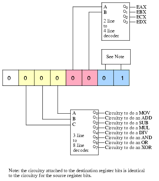
Figure 5.1 Separating an Opcode into Separate Fields to Ease Decoding
Although Intel probably went a little overboard with the design of the original 8086 instruction set, an important design goal is to keep instruction sizes within a reasonable range. CPUs with unnecessarily long instructions consume extra memory for their programs. This tends to create more cache misses and, therefore, hurts the overall performance of the CPU. Therefore, we would like our instructions to be as compact as possible so our programs' code uses as little memory as possible.
It would seem that if we are encoding 2n different instructions using n bits, there would be very little leeway in choosing the size of the instruction. It's going to take n bits to encode those 2n instructions, you can't do it with any fewer. You may, of course, use more than n bits; and believe it or not, that's the secret to reducing the size of a typical program on the CPU.
Before discussing how to use longer instructions to generate shorter programs, a short digression is necessary. The first thing to note is that we generally cannot choose an arbitrary number of bits for our opcode length. Assuming that our CPU is capable of reading bytes from memory, the opcode will probably have to be some even multiple of eight bits long. If the CPU is not capable of reading bytes from memory (e.g., most RISC CPUs only read memory in 32 or 64 bit chunks) then the opcode is going to be the same size as the smallest object the CPU can read from memory at one time (e.g., 32 bits on a typical RISC chip). Any attempt to shrink the opcode size below this data bus enforced lower limit is futile. Since we're discussing the 80x86 architecture in this text, we'll work with opcodes that must be an even multiple of eight bits long.
Another point to consider here is the size of an instruction's operands. Some CPU designers (specifically, RISC designers) include all operands in their opcode. Other CPU designers (typically CISC designers) do not count operands like immediate constants or address displacements as part of the opcode (though they do usually count register operand encodings as part of the opcode). We will take the CISC approach here and not count immediate constant or address displacement values as part of the actual opcode.
With an eight-bit opcode you can only encode 256 different instructions. Even if we don't count the instruction's operands as part of the opcode, having only 256 different instructions is somewhat limiting. It's not that you can't build a CPU with an eight-bit opcode, most of the eight-bit processors predating the 8086 had eight-bit opcodes, it's just that modern processors tend to have far more than 256 different instructions. The next step up is a two-byte opcode. With a two-byte opcode we can have up to 65,536 different instructions (which is probably enough) but our instructions have doubled in size (not counting the operands, of course).
If reducing the instruction size is an important design goal3 we can employ some techniques from data compression theory to reduce the average size of our instructions. The basic idea is this: first we analyze programs written for our CPU (or a CPU similar to ours if no one has written any programs for our CPU) and count the number of occurrences of each opcode in a large number of typical applications. We then create a sorted list of these opcodes from most-frequently-used to least-frequently-used. Then we attempt to design our instruction set using one-byte opcodes for the most-frequently-used instructions, two-byte opcodes for the next set of most-frequently-used instructions, and three (or more) byte opcodes for the rarely used instructions. Although our maximum instruction size is now three or more bytes, most of the actual instructions appearing in a program will use one or two byte opcodes, so the average opcode length will be somewhere between one and two bytes (let's call it 1.5 bytes) and a typical program will be shorter than had we chosen a two byte opcode for all instructions (see Figure 5.2).
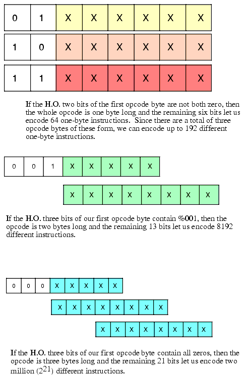
Figure 5.2 Encoding Instructions Using a Variable-Length Opcode
Although using variable-length instructions allows us to create smaller programs, it comes at a price. First of all, decoding the instructions is a bit more complicated. Before decoding an instruction field, the CPU must first decode the instruction's size. This extra step consumes time and may affect the overall performance of the CPU (by introducing delays in the decoding step and, thereby, limiting the maximum clock frequency of the CPU). Another problem with variable length instructions is that it makes decoding multiple instructions in a pipeline quite difficult (since we cannot trivially determine the instruction boundaries in the prefetch queue). These reasons, along with some others, is why most popular RISC architectures avoid variable-sized instructions. However, for our purpose, we'll go with a variable length approach since saving memory is an admirable goal.
Before actually choosing the instructions you want to implement in your CPU, now would be a good time to plan for the future. Undoubtedly, you will discover the need for new instructions at some point in the future, so reserving some opcodes specifically for that purpose is a real good idea. If you were using the instruction encoding appearing in Figure 5.2 for your opcode format, it might not be a bad idea to reserve one block of 64 one-byte opcodes, half (4,096) of the two-byte instructions, and half (1,048,576) of the three-byte opcodes for future use. In particular, giving up 64 of the very valuable one-byte opcodes may seem extravagant, but history suggests that such foresight is rewarded.
The next step is to choose the instructions you want to implement. Note that although we've reserved nearly half the instructions for future expansion, we don't actually have to implement instructions for all the remaining opcodes. We can choose to leave a good number of these instructions unimplemented (and effectively reserve them for the future as well). The right approach is not to see how quickly we can use up all the opcodes, but rather to ensure that we have a consistent and complete instruction set given the compromises we have to live with (e.g., silicon limitations). The main point to keep in mind here is that it's much easier to add an instruction later than it is to remove an instruction later. So for the first go-around, it's generally better to go with a simpler design rather than a more complex design.
The first step is to choose some generic instruction types. For a first attempt, you should limit the instructions to some well-known and common instructions. The best place to look for help in choosing these instructions is the instruction sets of other processors. For example, most processors you find will have instructions like the following:
Data movement instructions (e.g., MOV)
Arithmetic and logical instructions (e.g., ADD, SUB, AND, OR, NOT)
A set of conditional jump instructions (generally used after the compare instructions)
Other miscellaneous instructions
Your goal as the designer of the CPU's initial instruction set is to chose a reasonable set of instructions that will allow programmers to efficiently write programs (using as few instructions as possible) without adding so many instructions you exceed your silicon budget or violate other system compromises. This is a very strategic decision, one that CPU designers should base on careful research, experimentation, and simulation. The job of the CPU designer is not to create the best instruction set, but to create an instruction set that is optimal given all the constraints.
Once you've decided which instructions you want to include in your (initial) instruction set, the next step is to assign opcodes for them. The first step is to group your instructions into sets by common characteristics of those instructions. For example, an ADD instruction is probably going to support the exact same set of operands as the SUB instruction. So it makes sense to put these two instructions into the same group. On the other hand, the NOT instruction generally requires only a single operand4 as does a NEG instruction. So you'd probably put these two instructions in the same group but a different group than ADD and SUB.
Once you've grouped all your instructions, the next step is to encode them. A typical encoding will use some bits to select the group the instruction falls into, it will use some bits to select a particular instruction from that group, and it will use some bits to determine the types of operands the instruction allows (e.g., registers, memory locations, and constants). The number of bits needed to encode all this information may have a direct impact on the instruction's size, regardless of the frequency of the instruction. For example, if you need two bits to select a group, four bits to select an instruction within that group, and six bits to specify the instruction's operand types, you're not going to fit this instruction into an eight-bit opcode. On the other hand, if all you really want to do is push one of eight different registers onto the stack, you can use four bits to select the PUSH instruction and three bits to select the register (assuming the encoding in Figure 5.2 the eighth and H.O. bit would have to contain zero).
Encoding operands is always a problem because many instructions allow a large number of operands. For example, the generic 80x86 MOV instruction requires a two-byte opcode5. However, Intel noticed that the "mov( disp, eax );" and "mov( eax, disp );" instructions occurred very frequently. So they created a special one byte version of this instruction to reduce its size and, therefore, the size of those programs that use this instruction frequently. Note that Intel did not remove the two-byte versions of these instructions. They have two different instructions that will store EAX into memory or load EAX from memory. A compiler or assembler would always emit the shorter of the two instructions when given an option of two or more instructions that wind up doing exactly the same thing.
Notice an important trade-off Intel made with the MOV instruction. They gave up an extra opcode in order to provide a shorter version of one of the MOV instructions. Actually, Intel used this trick all over the place to create shorter and easier to decode instructions. Back in 1978 this was a good compromise (reducing the total number of possible instructions while also reducing the program size). Today, a CPU designer would probably want to use those redundant opcodes for a different purpose, however, Intel's decision was reasonable at the time (given the high cost of memory in 1978).
To further this discussion, we need to work with an example. So the next section will go through the process of designing a very simple instruction set as a means of demonstrating this process.
The Y86 Hypothetical Processor
Because of enhancements made to the 80x86 processor family over the years, Intel's design goals in 1978, and advances in computer architecture occurring over the years, the encoding of 80x86 instructions is very complex and somewhat illogical. Therefore, the 80x86 is not a good candidate for an example architecture when discussing how to design and encode an instruction set. However, since this is a text about 80x86 assembly language programming, attempting to present the encoding for some simpler real-world processor doesn't make sense. Therefore, we will discuss instruction set design in two stages: first, we will develop a simple (trivial) instruction set for a hypothetical processor that is a small subset of the 80x86, then we will expand our discussion to the full 80x86 instruction set. Our hypothetical processor is not a true 80x86 CPU, so we will call it the Y86 processor to avoid any accidental association with the Intel x86 family.
The Y86 processor is a very stripped down version of the x86 CPUs. First of all, the Y86 only supports one operand size - 16 bits. This simplification frees us from having to encode the size of the operand as part of the opcode (thereby reducing the total number of opcodes we will need). Another simplification is that the Y86 processor only supports four 16-bit registers: AX, BX, CX, and DX. This lets us encode register operands with only two bits (versus the three bits the 80x86 family requires to encode eight registers). Finally, the Y86 processors only support a 16-bit address bus with a maximum of 65,536 bytes of addressable memory. These simplifications, plus a very limited instruction set will allow us to encode all Y86 instructions using a single byte opcode and a two-byte displacement/offset (if needed).
The Y86 CPU provides 20 instructions. Seven of these instructions have two operands, eight of these instructions have a single operand, and five instructions have no operands at all. The instructions are MOV (two forms), ADD, SUB, CMP, AND, OR, NOT, JE, JNE, JB, JBE, JA, JAE, JMP, BRK, IRET, HALT, GET, and PUT. The following paragraphs describe how each of these work.
The MOV instruction is actually two instruction classes merged into the same instruction. The two forms of the mov instruction take the following forms:
mov( reg/memory/constant, reg );
where reg is any of AX, BX, CX, or DX; constant is a numeric constant (using hexadecimal notation), and memory is an operand specifying a memory location. The next section describes the possible forms the memory operand can take. The "reg/memory/constant" operand tells you that this particular operand may be a register, memory location, or a constant.
The arithmetic and logical instructions take the following forms:
add( reg/memory/constant, reg );
sub( reg/memory/constant, reg );
cmp( reg/memory/constant, reg );
and( reg/memory/constant, reg );
or( reg/memory/constant, reg );
Note: the NOT instruction appears separately because it is in a different class than the other arithmetic instructions (since it supports only a single operand).
The ADD instruction adds the value of the first operand to the second (register) operand, leaving the sum in the second (register) operand. The SUB instruction subtracts the value of the first operand from the second, leaving the difference in the second operand. The CMP instruction compares the first operand against the second and saves the result of this comparison for use with one of the conditional jump instructions (described in a moment). The AND and OR instructions compute the corresponding bitwise logical operation on the two operands and store the result into the first operand. The NOT instruction inverts the bits in the single memory or register operand.
The control transfer instructions interrupt the sequential execution of instructions in memory and transfer control to some other point in memory either unconditionally, or after testing the result of the previous CMP instruction. These instructions include the following:
ja dest; -- Jump if above (i.e., greater than)
jae dest; -- Jump if above or equal (i.e., greater than or equal)
jb dest; -- Jump if below (i.e., less than)
jbe dest; -- Jump if below or equal (i.e., less than or equal)
jne dest; -- Jump if not equal
jmp dest; -- Unconditional jump
iret; -- Return from an interrupt
The first six instructions let you check the result of the previous CMP instruction for greater than, greater or equal, less than, less or equal, equality, or inequality6. For example, if you compare the AX and BX registers with a "cmp( ax, bx );" instruction and execute the JA instruction, the Y86 CPU will jump to the specified destination location if AX was greater than BX. If AX was not greater than BX, control will fall through to the next instruction in the program.
The JMP instruction unconditionally transfers control to the instruction at the destination address. The IRET instruction returns control from an interrupt service routine, which we will discuss later.
The GET and PUT instructions let you read and write integer values. GET will stop and prompt the user for a hexadecimal value and then store that value into the AX register. PUT displays (in hexadecimal) the value of the AX register.
The remaining instructions do not require any operands, they are HALT and BRK. HALT terminates program execution and BRK stops the program in a state that it can be restarted.
The Y86 processors require a unique opcode for every different instruction, not just the instruction classes. Although "mov( bx, ax );" and "mov( cx, ax );" are both in the same class, they must have different opcodes if the CPU is to differentiate them. However, before looking at all the possible opcodes, perhaps it would be a good idea to learn about all the possible operands for these instructions.
5.3.1 Addressing Modes on the Y86
The Y86 instructions use five different operand types: registers, constants, and three memory addressing schemes. Each form is called an addressing mode. The Y86 processor supports the register addressing mode7, the immediate addressing mode, the indirect addressing mode, the indexed addressing mode, and the direct addressing mode. The following paragraphs explain each of these modes.
Register operands are the easiest to understand. Consider the following forms of the MOV instruction:
The first instruction accomplishes absolutely nothing. It copies the value from the AX register back into the AX register. The remaining three instructions copy the values of BX, CX and DX into AX. Note that these instructions leave BX, CX, and DX unchanged. The second operand (the destination) is not limited to AX; you can move values to any of these registers.
Constants are also pretty easy to deal with. Consider the following instructions:
These instructions are all pretty straightforward; they load their respective registers with the specified hexadecimal constant8.
There are three addressing modes which deal with accessing data in memory. The following instructions demonstrate the use of these addressing modes:
The first instruction above uses the direct addressing mode to load AX with the 16 bit value stored in memory starting at location $1000.
The "mov( [bx], ax );" instruction loads AX from the memory location specified by the contents of the bx register. This is an indirect addressing mode. Rather than using the value in BX, this instruction accesses to the memory location whose address appears in BX. Note that the following two instructions:
are equivalent to the single instruction:
Of course, the second sequence is preferable. However, there are many cases where the use of indirection is faster, shorter, and better. We'll see some examples of this a little later.
The last memory addressing mode is the indexed addressing mode. An example of this memory addressing mode is
This instruction adds the contents of BX with $1000 to produce the address of the memory value to fetch. This instruction is useful for accessing elements of arrays, records, and other data structures.
5.3.2 Encoding Y86 Instructions
Although we could arbitrarily assign opcodes to each of the Y86 instructions, keep in mind that a real CPU uses logic circuitry to decode the opcodes and act appropriately on them. A typical CPU opcode uses a certain number of bits in the opcode to denote the instruction class (e.g., MOV, ADD, SUB), and a certain number of bits to encode each of the operands.
A typical Y86 instruction takes the form shown in Figure 5.3. The basic instruction is either one or three bytes long. The instruction opcode consists of a single byte that contains three fields. The first field, the H.O. three bits, defines the instruction. This provides eight combinations. As you may recall, there are 20 different instructions; we cannot encode 20 instructions with three bits, so we'll have to pull some tricks to handle the other instructions. As you can see in Figure 5.3, the basic opcode encodes the MOV instructions (two instructions, one where the rr field specifies the destination, one where the mmm field specifies the destination), and the ADD, SUB, CMP, AND, and OR instructions. There is one additional instruction field: special. The special instruction class provides a mechanism that allows us to expand the number of available instruction classes, we will return to this expansion opcode shortly.
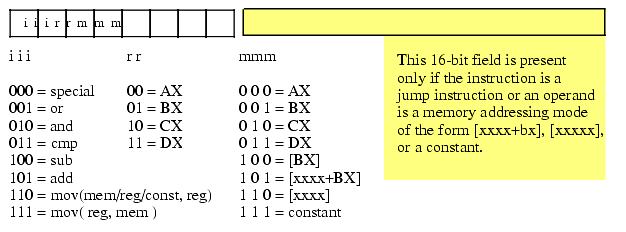
Figure 5.3 Basic Y86 Instruction Encoding
To determine a particular instruction's opcode, you need only select the appropriate bits for the iii, rr, and mmm fields. The rr field contains the destination register (except for the MOV instruction whose iii field is %111) and the mmm field encodes the source operand. For example, to encode the "mov( bx, ax );" instruction you would select iii=110 ("mov( reg, reg );), rr=00 (AX), and mmm=001 (BX). This produces the one-byte instruction %11000001 or $C0.
Some Y86 instructions require more than one byte. For example, the instruction "mov( [1000], ax );" loads the AX register from memory location $1000. The encoding for the opcode is %11000110 or $C6. However, the encoding for the "mov( [2000], ax );" instruction's opcode is also $C6. Clearly these two instructions do different things, one loads the AX register from memory location $1000 while the other loads the AX register from memory location $2000. To encode an address for the [xxxx] or [xxxx+bx] addressing modes, or to encode the constant for the immediate addressing mode, you must follow the opcode with the 16-bit address or constant, with the L.O. byte immediately following the opcode in memory and the H.O. byte after that. So the three byte encoding for "mov( [1000], ax );" would be $C6, $00, $10 and the three byte encoding for "mov( [2000], ax );" would be $C6, $00, $20.
The special opcode allows the x86 CPU to expand the set of available instructions. This opcode handles several zero and one-operand instructions as shown in Figure 5.4 and Figure 5.5.
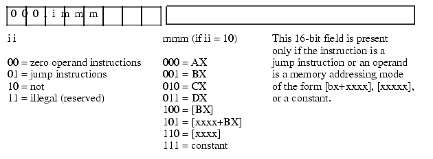
Figure 5.4 Single Operand Instruction Encodings
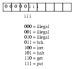
Figure 5.5 Zero Operand Instruction Encodings
There are four one-operand instruction classes. The first encoding (00) further expands the instruction set with a set of zero-operand instructions (see Figure 5.5). The second opcode is also an expansion opcode that provides all the Y86 jump instructions (see Figure 5.6). The third opcode is the NOT instruction. This is the bitwise logical not operation that inverts all the bits in the destination register or memory operand. The fourth single-operand opcode is currently unassigned. Any attempt to execute this opcode will halt the processor with an illegal instruction error. CPU designers often reserve unassigned opcodes like this one to extend the instruction set at a future date (as Intel did when moving from the 80286 processor to the 80386).
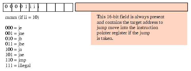
Figure 5.6 Jump Instruction Encodings
There are seven jump instructions in the x86 instruction set. They all take the following form:
The JMP instruction copies the 16-bit value (address) following the opcode into the IP register. Therefore, the CPU will fetch the next instruction from this target address; effectively, the program "jumps" from the point of the JMP instruction to the instruction at the target address.
The JMP instruction is an example of an unconditional jump instruction. It always transfers control to the target address. The remaining six instructions are conditional jump instructions. They test some condition and jump if the condition is true; they fall through to the next instruction if the condition is false. These six instructions, JA, JAE, JB, JBE, JE, and JNE let you test for greater than, greater than or equal, less than, less than or equal, equality, and inequality. You would normally execute these instructions immediately after a CMP instruction since it sets the less than and equality flags that the conditional jump instructions test. Note that there are eight possible jump opcodes, but the x86 uses only seven of them. The eighth opcode is another illegal opcode.
The last group of instructions, the zero operand instructions, appear in Figure 5.5. Three of these instructions are illegal instruction opcodes. The BRK (break) instruction pauses the CPU until the user manually restarts it. This is useful for pausing a program during execution to observe results. The IRET (interrupt return) instruction returns control from an interrupt service routine. We will discuss interrupt service routines later. The HALT program terminates program execution. The GET instruction reads a hexadecimal value from the user and returns this value in the AX register; the PUT instruction outputs the value in the AX register.
5.3.3 Hand Encoding Instructions
Keep in mind that the Y86 processor fetches instructions as bit patterns from memory. It decodes and executes those bit patterns. The processor does not execute instructions of the form "mov( ax, bx );" (that is, a string of characters that are readable by humans). Instead, it executes the bit pattern $C1 from memory. Instructions like "mov( ax, bx );" and "add( 5, cx );" are human-readable representations of these instructions that we must first convert into machine code (that is, the binary representation of the instruction that the machine actually executes). In this section we will explore how to manually accomplish this task.
The first step is to chose an instruction to convert into machine code. We'll start with a very simple example, the "add( cx, dx );" instruction. Once you've chosen the instruction, you look up the instruction in one of the figures of the previous section. The ADD instruction is in the first group (see Figure 5.3) and has an iii field of %101. The source operand is CX, so the mmm field is %010 and the destination operand is DX so the rr field is %11. Merging these bits produces the opcode %10111010 or $BA.
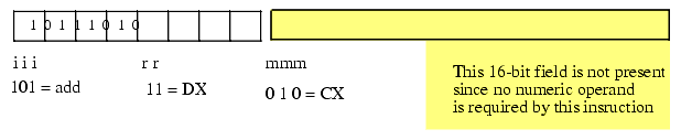
Figure 5.7 Encoding ADD( cx, dx );
Now consider the "add( 5, ax );" instruction. Since this instruction has an immediate source operand, the mmm field will be %111. The destination register operand is AX (%00) so the full opcode becomes $10100111 or $A7. Note, however, that this does not complete the encoding of the instruction. We also have to include the 16-bit constant $0005 as part of the instruction. The binary encoding of the constant must immediately follow the opcode in memory, so the sequence of bytes in memory (from lowest address to highest address) is $A7, $05, $00. Note that the L.O. byte of the constant follows the opcode and the H.O. byte of the constant follows the L.O. byte. This sequence appears backwards because the bytes are arranged in order of increasing memory address and the H.O. byte of a constant always appears in the highest memory address.
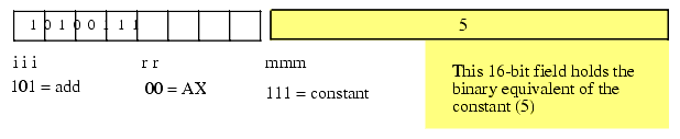
Figure 5.8 Encoding ADD( 5, ax );
The "add( [2ff+bx], cx );" instruction also contains a 16-bit constant associated with the instruction's encoding - the displacement portion of the indexed addressing mode. To encode this instruction we use the following field values: iii=%101, rr=%10, and mmm=%101. This produces the opcode byte %10110101 or $B5. The complete instruction also requires the constant $2FF so the full instruction is the three-byte sequence $B5, $FF, $02.
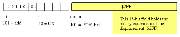
Figure 5.9 Encoding ADD( [$2ff+bx], cx );
Now consider the "add( [1000], ax );" instruction. This instruction adds the 16-bit contents of memory locations $1000 and $1001 to the value in the AX register. Once again, iii=%101 for the ADD instruction. The destination register is AX so rr=%00. Finally, the addressing mode is the displacement-only addressing mode, so mmm=%110. This forms the opcode %10100110 or $A6. The instruction is three bytes long since it must encode the displacement (address) of the memory location in the two bytes following the opcode. Therefore, the complete three-byte sequence is $A6, $00, $10.
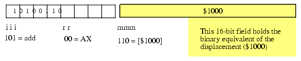
Figure 5.10 Encoding ADD( [1000], ax );
The last addressing mode to consider is the register indirect addressing mode, [bx]. The "add( [bx], bx );" instruction uses the following encoded values: mmm=%101, rr=%01 (bx), and mmm=%100 ([bx]). Since the value in the BX register completely specifies the memory address, there is no need for a displacement field. Hence, this instruction is only one byte long.
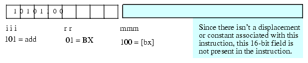
Figure 5.11 Encoding the ADD( [bx], bx ); Instruction
You use a similar approach to encode the SUB, CMP, AND, and OR instructions as you do the ADD instruction. The only difference is that you use different values for the iii field in the opcode.
The MOV instruction is special because there are two forms of the MOV instruction. You encode the first form (iii=%110) exactly as you do the ADD instruction. This form copies a constant or data from memory or a register (the mmm field) into a destination register (the rr field).
The second form of the MOV instruction (iii=%111) copies data from a source register (rr) to a destination memory location (that the mmm field specifies). In this form of the MOV instruction, the source/destination meanings of the rr and mmm fields are reversed so that rr is the source field and mmm is the destination field. Another difference is that the mmm field may only contain the values %100 ([bx]), %101 ([disp+bx]), and %110 ([disp]). The destination values cannot be %000..%011 (registers) or %111 (constant). These latter five encodings are illegal (the register destination instructions are handled by the other MOV instruction and storing data into a constant doesn't make any sense).
The Y86 processor supports a single instruction with a single memory/register operand - the NOT instruction. The NOT instruction has the syntax: "not( reg );" or "not( mem );" where mem represents one of the memory addressing modes ([bx], [disp+bx], or [disp]). Note that you may not specify a constant as the operand of the NOT instruction.
Since the NOT instruction has only a single operand, it only uses the mmm field to encode this operand. The rr field, combined with the iii field, selects the NOT instruction (iii=%000 and rr=%10). Whenever the iii field contains zero this tells the CPU that special decoding is necessary for the instruction. In this case, the rr field specifies whether we have the NOT instruction or one of the other specially decoded instructions.
To encode an instruction like "not( ax );" you would simply specify %000 for iii and %10 for the rr fields. Then you would encode the mmm field the same way you would encode this field for the ADD instruction. Since mmm=%000 for AX, the encoding of "not( ax );" would be %00010000 or $10.
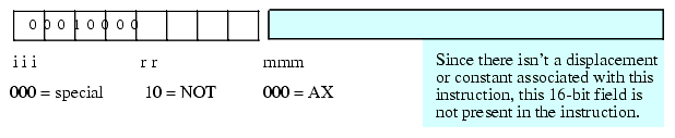
Figure 5.12 Encoding the NOT( ax ); Instruction
The NOT instruction does not allow an immediate (constant) operand, hence the opcode %00010111 ($17) is an illegal opcode.
The Y86 conditional jump instructions also use a special encoding. These instructions are always three bytes long. The first byte (the opcode) specifies which conditional jump instruction to execute and the next two bytes specify where the CPU transfers if the condition is met. There are seven different Y86 jump instructions, six conditional jumps and one unconditional jump. These instructions set mmm=%000, rr=%01, and use the mmm field to select one of the seven possible jumps; the eighth possible opcode is an illegal opcode (see Figure 5.6). Encoding these instructions is relatively straight-forward. Once you pick the instruction you want to encode, you've determined the opcode (since there is a single opcode for each instruction). The opcode values fall in the range $08..$0E ($0F is the illegal opcode).
The only field that requires some thought is the 16-bit operand that follows the opcode. This field holds the address of the target instruction to which the (un)conditional jump transfers if the condition is true (e.g., JE transfers control to this address if the previous CMP instruction found that its two operands were equal). To properly encode this field you must know the address of the opcode byte of the target instruction. If you've already converted the instruction to binary form and stored it into memory, this isn't a problem; just specify the address of that instruction as the operand of the condition jump. On the other hand, if you haven't yet written, converted, and placed that instruction into memory, knowing its address would seem to require a bit of divination. Fortunately, you can figure out the target address by computing the lengths of all the instructions between the current jump instruction you're encoding and the target instruction. Unfortunately, this is an arduous task. The best solution is to write all your instructions down on paper, compute their lengths (which is easy, all instructions are one or three bytes long depending on the presence of a 16-bit operand), and then assign an appropriate address to each instruction. Once you've done this (and, assuming you haven't made any mistakes) you'll know the starting address for each instruction and you can fill in target address operands in your (un)conditional jump instructions as you encode them. Fortunately, there is a better way to do this, as you'll see in the next section.
The last group of instructions, the zero operand instructions, are the easiest to encode. Since they have no operands they are always one byte long and the instruction uniquely specifies the opcode for the instruction. These instructions always have iii=%000, rr=%00, and mmm specifies the particular instruction opcode (see Figure 5.5). Note that the Y86 CPU leaves three of these instructions undefined (so we can use these opcodes for future expansion).
5.3.4 Using an Assembler to Encode Instructions
Of course, hand coding machine language programs as demonstrated in the previous section is impractical for all but the smallest programs. Certainly you haven't had to do anything like this when writing HLA programs. The HLA compiler lets you create a text file containing human readable forms of the instructions. You might wonder why we can write such code for the 80x86 but not for the Y86. The answer is to use an assembler or compiler for the Y86. The job of an assembler/compiler is to read a text file containing human readable text and translate that text into the binary encoded representation for the corresponding machine language program.
An assembler or compiler is nothing special. It's just another program that executes on your computer system. The only thing special about an assembler or compiler is that it translates programs from one form (source code) to another (machine code). A typical Y86 assembler, for example, would read lines of text with each line containing a Y86 instruction, it would parse9 each statement and then write the binary equivalent of each instruction to memory or to a file for later execution.
Assemblers have two big advantages over coding in machine code. First, they automatically translate strings like "ADD( ax, bx );" and "MOV( ax, [1000]);" to their corresponding binary form. Second, and probably even more important, assemblers let you attach labels to statements and refer to those labels within jump instructions; this means that you don't have to know the target address of an instruction in order to specify that instruction as the target of a jump or conditional jump instruction. Windows users have access to a very simple Y86 assembler10 that lets you specify up to 26 labels in a program (using the symbols 'A'..'Z'). To attach a label to a statement, you simply preface the instruction with the label and a colon, e.g.,
To transfer control to a statement with a label attached to it, you simply specify the label name as the operand of the jump instruction, e.g.,
The assembler will compute the address of the label and fill in the address for you whenever you specify the label as the operand of a jump or conditional jump instruction. The assembler can do this even if it hasn't yet encountered the label in the program's source file (i.e., the label is attached to a later instruction in the source file). Most assemblers accomplish this magic by making two passes over the source file. During the first pass the assembler determines the starting address of each symbol and stores this information in a simple database called the symbol table. The assembler does not emit any machine code during this first pass. Then the assembler makes a second pass over the source file and actually emits the machine code. During this second pass it looks up all label references in the symbol table and uses the information it retrieves from this database to fill in the operand fields of the instructions that refer to some symbol.
5.3.5 Extending the Y86 Instruction Set
The Y86 CPU is a trivial CPU, suitable only for demonstrating how to encode machine instructions. However, like any good CPU the Y86 design does provide the capability for expansion. So if you wanted to improve the CPU by adding new instructions, the ability to accomplish this exists in the instruction set.
There are two standard ways to increase the number of instructions in a CPU's instruction set. Both mechanisms require the presence of undefined (or illegal) opcodes on the CPU. Since the Y86 CPU has several of these, we can expand the instruction set.
The first method is to directly use the undefined opcodes to define new instructions. This works best when there are undefined bit patterns within an opcode group and the new instruction you want to add falls into that same group. For example, the opcode %00011mmm falls into the same group as the NOT instruction. If you decided that you really needed a NEG (negate, take the two's complement) instruction, using this particular opcode for this purpose makes a lot of sense because you'd probably expect the NEG instruction to use the same syntax (and, therefore, decoding) as the NOT instruction.
Likewise, if you want to add a zero-operand instruction to the instruction set, there are three undefined zero-operand instructions that you could use for this purpose. You'd just appropriate one of these opcodes and assign your instruction to it.
Unfortunately, the Y86 CPU doesn't have that many illegal opcodes open. For example, if you wanted to add the SHL, SHR, ROL, and ROR instructions (shift and rotate left and right) as single-operand instructions, there is insufficient space in the single operand instruction opcodes to add these instructions (there is currently only one open opcode you could use). Likewise, there are no two-operand opcodes open, so if you wanted to add an XOR instruction or some other two-operand instruction, you'd be out of luck.
A common way to handle this dilemma (one the Intel designers have employed) is to use a prefix opcode byte. This opcode expansion scheme uses one of the undefined opcodes as an opcode prefix byte. Whenever the CPU encounters a prefix byte in memory, it reads and decodes the next byte in memory as the actual opcode. However, it does not treat this second byte as it would any other opcode. Instead, this second opcode byte uses a completely different encoding scheme and, therefore, lets you specify as many new instructions as you can encode in that byte (or bytes, if you prefer). For example, the opcode $FF is illegal (it corresponds to a "mov( dx, const );" instruction) so we can use this byte as a special prefix byte to further expand the instruction set11.
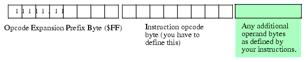
Figure 5.13 Using a Prefix Byte to Extend the Instruction Set
5.4 Encoding 80x86 Instructions
The Y86 processor is simple to understand, easy to hand encode instructions for it, and a great vehicle for learning how to assign opcodes. It's also a purely hypothetical device intended only as a teaching tool Therefore, you can now forget all about the Y86, it's served its purpose. Now it's time to take a look that the actual machine instruction format for the 80x86 CPU family.
They don't call the 80x86 CPU a Complex Instruction Set Computer for nothing. Although more complex instruction encodings do exist, no one is going to challenge the assertion that the 80x86 has a complex instruction encoding. The generic 80x86 instruction takes the form shown in Figure 5.14. Although this diagram seems to imply that instructions can be up to 16 bytes long, in actuality the 80x86 will not allow instructions greater than 15 bytes in length.
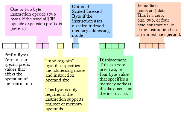
Figure 5.14 80x86 Instruction Encoding
The prefix bytes are not the "opcode expansion prefix" that the previous sections in this chapter discussed. Instead, these are special bytes to modify the behavior of existing instructions (rather than define new instructions). We'll take a look at a couple of these prefix bytes in a little bit, others we'll leave for discussion in later chapters. The 80x86 certainly supports more than four prefix values, however, an instruction may have a maximum of four prefix bytes attached to it. Also note that the behavior of many prefix bytes are mutually exclusive and the results are undefined if you put a pair of mutually exclusive prefix bytes in front of an instruction.
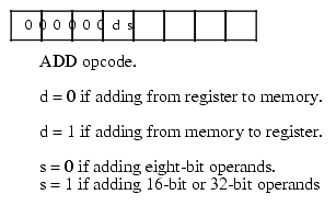
The 80x86 supports two basic opcode sizes: a standard one-byte opcode and a two-byte opcode consisting of a $0F opcode expansion prefix byte and a second byte specifying the actual instruction. One way to view these opcode bytes is as an eight-bit extension of the iii field in the Y86 encoding. This provides for up to 512 different instruction classes (although the 80x86 does not yet use them all). In reality, various instruction classes use certain bits in this opcode for decidedly non-instruction-class purposes. For example, consider the ADD instruction opcode. It takes the form shown in Figure 5.15.
Note that bit number zero specifies the size of the operands the ADD instruction operates upon. If this field contains zero then the operands are eight bit registers and memory locations. If this bit contains one then the operands are either 16-bits or 32-bits. Under 32-bit operating systems the default is 32-bit operands if this field contains a one. To specify a 16-bit operand (under Windows or Linux) you must insert a special "operand-size prefix byte" in front of the instruction.
Bit number one specifies the direction of the transfer. If this bit is zero, then the destination operand is a memory location (e.g., "add( al, [ebx]);" If this bit is one, then the destination operand is a register (e.g., "add( [ebx], al );" You'll soon see that this direction bit creates a problem that results in one instruction have two different possible opcodes.
5.4.1 Encoding Instruction Operands
The "mod-reg-r/m" byte (in Figure 5.14) specifies a basic addressing mode. This byte contains the following fields:
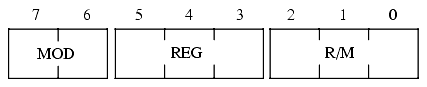
The REG field specifies an 80x86 register. Depending on the instruction, this can be either the source or the destination operand. Many instructions have the "d" (direction) field in their opcode to choose whether this operand is the source (d=0) or the destination (d=1) operand. This field is encoded using the bit patterns found in the following table:
For certain (single operand) instructions, the REG field may contain an opcode extension rather than a register value (the R/M field will specify the operand in this case).
The MOD and R/M fields combine to specify the other operand in a two-operand instruction (or the only operand in a single-operand instruction like NOT or NEG). Remember, the "d" bit in the opcode determines which operand is the source and which is the destination. The MOD and R/M fields together specify the following addressing modes:
There are a couple of interesting things to note about this table. First of all, note that there are two forms of the [reg+disp] addressing modes: one form with an eight-bit displacement and one form with a 32-bit displacement. Addressing modes whose displacement falls in the range -128..+127 require only a single byte displacement after the opcode; hence these instructions will be shorter (and sometimes faster) than instructions whose displacement value is outside this range. It turns out that many offsets are within this range, so the assembler/compiler can generate shorter instructions for a large percentage of the instructions.
The second thing to note is that there is no [ebp] addressing mode. If you look in the table above where this addressing mode logically belongs, you'll find that it's slot is occupied by the 32-bit displacement only addressing mode. The basic encoding scheme for addressing modes didn't allow for a displacement only addressing mode, so Intel "stole" the encoding for [ebp] and used that for the displacement only mode. Fortunately, anything you can do with the [ebp] addressing mode you can do with the [ebp+disp8] addressing mode by setting the eight-bit displacement to zero. True, the instruction is a little bit longer, but the capabilities are still there. Intel (wisely) chose to replace this addressing mode because they anticipated that programmers would use this addressing mode less often than the other register indirect addressing modes (for reasons you'll discover in a later chapter).
Another thing you'll notice missing from this table are addressing modes of the form [ebx+edx*4], the so-called scaled indexed addressing modes. You'll also notice that the table is missing addressing modes of the form [esp], [esp+disp8], and [esp+disp32]. In the slots where you would normally expect these addressing modes you'll find the SIB (scaled index byte) modes. If these values appear in the MOD and R/M fields then the addressing mode is a scaled indexed addressing mode with a second byte (the SIB byte) following the MOD-REG-R/M byte that specifies the registers to use (note that the MOD field still specifies the displacement size of zero, one, or four bytes). The following diagram shows the layout of this SIB byte and the following tables explain the values for each field.
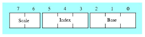
Figure 5.17 SIB (Scaled Index Byte) Layout
The MOD-REG-R/M and SIB bytes are complex and convoluted, no question about that. The reason these addressing mode bytes are so convoluted is because Intel reused their 16-bit addressing circuitry in the 32-bit mode rather than simply abandoning the 16-bit format in the 32-bit mode. There are good hardware reasons for this, but the end result is a complex scheme for specifying addressing modes.
Part of the reason the addressing scheme is so convoluted is because of the special cases for the SIB and displacement-only modes. You will note that the intuitive encoding of the MOD-REG-R/M byte does not allow for a displacement-only mode. Intel added a quick kludge to the addressing scheme replacing the [EBP] addressing mode with the displacement-only mode. Programmers who actually want to use the [EBP] addressing mode have to use [EBP+0] instead. Semantically, this mode produces the same result but the instruction is one byte longer since it requires a displacement byte containing zero.
You will also note that if the REG field of the MOD-REG-R/M byte contains %100 and MOD does not contain %11 then the addressing mode is an "SIB" mode rather than the expected [ESP], [ESP+disp8], or [ESP+disp32] mode. The SIB mode is used when an addressing mode uses one of the scaled indexed registers, i.e., one of the following addressing modes:
[reg32+ebx*n] Note: n = 1, 2, 4, or 8.
[disp+eax*n] MOD = %00 and BASE field contains %101
In each of these addressing modes, the MOD field of the MOD-REG-R/M byte specifies the size of the displacement (zero, one, or four bytes). This is indicated via the modes "SIB Mode," "SIB + disp8 Mode," and "SIB + disp32 Mode." The Base and Index fields of the SIB byte select the base and index registers, respectively. Note that this addressing mode does not allow the use of the ESP register as an index register. Presumably, Intel left this particular mode undefined to provide the ability to extend the addressing modes in a future version of the CPU (although extending the addressing mode sequence to three bytes seems a bit extreme).
Like the MOD-REG-R/M encoding, the SIB format redefines the [EBP+index*scale] mode as a displacement plus index mode. Once again, if you really need this addressing mode, you will have to use a single byte displacement value containing zero to achieve the same result.
5.4.2 Encoding the ADD Instruction: Some Examples
To figure out how to encode an instruction using this complex scheme, some examples are warranted. So let's take a lot at how to encode the 80x86 ADD instruction using various addressing modes. The ADD opcode is $00, $01, $02, or $03, depending on the direction and size bits in the opcode (see Figure 5.15). The following figures each describe how to encode various forms of the ADD instruction using different addressing modes.
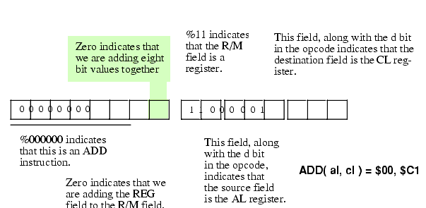
Figure 5.18 Encoding the ADD( al, cl ); Instruction
There is an interesting side effect of the operation of the direction bit and the MOD-REG-R/M organization: some instructions have two different opcodes (and both are legal). For example, we could encode the "add( al, cl );" instruction from Figure 5.18 as $02, $C8 by reversing the AL and CL registers in the REG and R/M fields and then setting the d bit in the opcode (bit #1). This issue applies to instructions with two register operands.
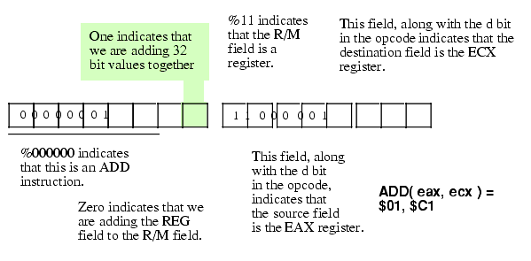
Figure 5.19 Encoding the ADD( eax, ecx ); instruction
Note that we can also encode "add( eax, ecx );" using the bytes $03, $C8.
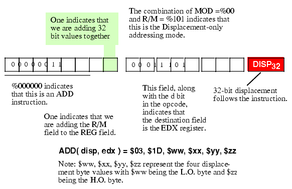
Figure 5.20 Encoding the ADD( disp, edx ); Instruction
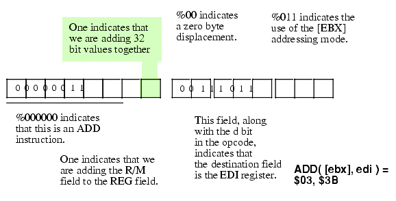
Figure 5.21 Encoding the ADD( [ebx], edi ); Instruction
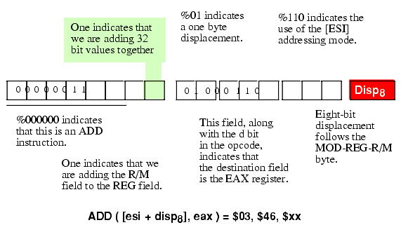
Figure 5.22 Encoding the ADD( [esi+disp8], eax ); Instruction
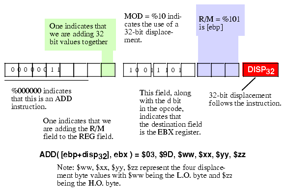
Figure 5.23 Encoding the ADD ( [ebp+disp32], ebx); Instruction
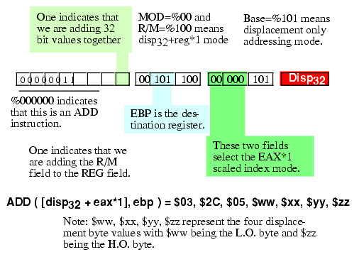
Figure 5.24 Encoding the ADD( [disp32 +eax*1], ebp ); Instruction
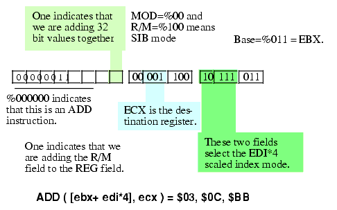
Figure 5.25 Encoding the ADD( [ebx + edi * 4], ecx ); Instruction
5.4.3 Encoding Immediate Operands
You may have noticed that the MOD-REG-R/M and SIB bytes don't contain any bit combinations you can use to specify an immediate operand. The 80x86 uses a completely different opcode to specify an immediate operand. Figure 5.26 shows the basic encoding for an ADD immediate instruction.
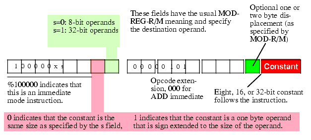
Figure 5.26 Encoding an ADD Immediate Instruction
There are three major differences between the encoding of the ADD immediate and the standard ADD instruction. First, and most important, the opcode has a one in the H.O. bit position. This tells the CPU that the instruction has an immediate constant. This individual change, however, does not tell the CPU that it must execute an ADD instruction, as you'll see momentarily.
The second difference is that there is no direction bit in the opcode. This makes sense because you cannot specify a constant as a destination operand. Therefore, the destination operand is always the location the MOD and R/M bits specify in the MOD-REG-R/M field.
In place of the direction bit, the opcode has a sign extension (x) bit. For eight-bit operands, the CPU ignores this bit. For 16-bit and 32-bit operands, this bit specifies the size of the constant following the ADD instruction. If this bit contains zero then the constant is the same size as the operand (i.e., 16 or 32 bits). If this bit contains one then the constant is a signed eight-bit value and the CPU sign extends this value to the appropriate size before adding it to the operand. This little trick often makes programs quite a bit shorter because one commonly adds small valued constants to 16 or 32 bit operands.
The third difference between the ADD immediate and the standard ADD instruction is the meaning of the REG field in the MOD-REG-R/M byte. Since the instruction implies that the source operand is a constant and the MOD-R/M fields specify the destination operand, the instruction does not need to use the REG field to specify an operand. Instead, the 80x86 CPU uses these three bits as an opcode extension. For the ADD immediate instruction these three bits must contain zero (other bit patterns would correspond to a different instruction).
Note that when adding a constant to a memory location, the displacement (if any) associated with the memory location immediately precedes the immediate (constant) data in the opcode sequence.
5.4.4 Encoding Eight, Sixteen, and Thirty-Two Bit Operands
When Intel designed the 8086 they used one bit (s) to select between eight and sixteen bit integer operand sizes in the opcode. Later, when they extended the 80x86 architecture to 32 bits with the introduction of the 80386, they had a problem, with this single bit they could only encode two sizes but they needed to encode three (8, 16, and 32 bits). To solve this problem, they used a operand size prefix byte.
Intel studied their instruction set and came to the conclusion that in a 32-bit environment, programs were more likely to use eight-bit and 32-bit operands far more often than 16-bit operands. So Intel decided to let the size bit (s) in the opcode select between eight and thirty-two bit operands, as the previous sections describe. Although modern 32-bit programs don't use 16-bit operands that often, they do need them now and then. To allow for 16-bit operands, Intel lets you prefix a 32-bit instruction with the operand size prefix byte, whose value is $66. This prefix byte tells the CPU to operand on 16-bit data rather than 32-bit data.
You do not have to explicitly put an operand size prefix byte in front of your 16-bit instructions; the assembler will take care of this automatically for you whenever you use a 16-bit operand in an instruction. However, do keep in mind that whenever you use a 16-bit operand in a 32-bit program, the instruction is longer (by one byte) because of the prefix value. Therefore, you should be careful about using 16-bit instructions if size (and to a lesser extent, speed) are important because these instructions are longer (and may be slower because of their effect on the cache).
5.4.5 Alternate Encodings for Instructions
As noted earlier in this chapter, one of Intel's primary design goals for the 80x86 was to create an instruction set to allow programmers to write very short programs in order to save precious (at the time) memory. One way they did this was to create alternate encodings of some very commonly used instructions. These alternate instructions were shorter than the standard counterparts and Intel hoped that programmers would make extensive use of these instructions, thus creating shorter programs.
A good example of these alternate instructions are the "add( constant, accumulator );" instructions (the accumulator is AL, AX, or EAX). The 80x86 provides a single byte opcode for "add( constant, al );" and "add( constant, eax );" (the opcodes are $04 and $05, respectively). With a one-byte opcode and no MOD-REG-R/M byte, these instructions are one byte shorter than their standard ADD immediate counterparts. Note that the "add( constant, ax );" instruction requires an operand size prefix (as does the standard "add( constant, ax );" instruction, so it's opcode is effectively two bytes if you count the prefix byte. This, however, is still one byte shorter than the corresponding standard ADD immediate.
You do not have to specify anything special to use these instructions. Any decent assembler will automatically choose the shortest possible instruction it can use when translating your source code into machine code. However, you should note that Intel only provides alternate encodings for the accumulator registers. Therefore, if you have a choice of several instructions to use and the accumulator registers are among these choices, the AL/AX/EAX registers almost always make the best bet. This is a good reason why you should take some time and scan through the encodings of the 80x86 instructions some time. By familiarizing yourself with the instruction encodings, you'll know which instructions have special (and, therefore, shorter) encodings.
5.5 Putting It All Together
Designing an instruction set that can stand the test of time is a true intellectual challenge. An engineer must balance several compromises when choosing an instruction set and assigning opcodes for the instructions. The Intel 80x86 instruction set is a classic example of a kludge that people are currently using for purposes the original designers never intended. However, the 80x86 is also a marvelous testament to the ingenuity of Intel's engineers who were faced with the difficult task of extending the CPU in ways it was never intended. The end result, though functional, is extremely complex. Clearly, no one designing a CPU (from scratch) today would choose the encoding that Intel's engineers are using. Nevertheless, the 80x86 CPU does demonstrate that careful planning (or just plain luck) does give the designer the ability to extend the CPU far beyond it's original design.
Historically, an important fact we've learned from the 80x86 family is that it's very poor planning to assume that your CPU will last only a short time period and that users will replace the chip and their software when something better comes along. Software developers usually don't have a problem adapting to a new architecture when they write new software (assuming financial incentive to do so), but they are very resistant to moving existing software from one platform to another. This is the primary reason the Intel 80x86 platform remains popular to this day.
Choosing which instructions you want to incorporate into the initial design of a new CPU is a difficult task. You must balance the desire to provide lots of useful instructions with the silicon budget and you must also be careful not to include lots of irrelevant instructions that programmers wind up ignoring for one reason or another. Remember, all future versions of the CPU will probably have to support all the instructions in the initial instruction set, so it's better to err on the side of supplying too few instructions rather than too many. Remember, you can always expand the instruction set in a later version of the chip.
Hand in hand with selecting the optimal instruction set is allowing for easy future expansion of the chip. You must leave some undefined opcodes available so you can easily expand the instruction set later on. However, you must balance the number of undefined opcodes with the number of initial instructions and the size of your opcodes. For efficiency reasons, we want the opcodes to be as short as possible. We also need a reasonable set of instructions in the initial instruction set. A reasonable instruction set may consume most of the legal bit patterns in small opcode. So a hard decision has to be made: reduce the number of instructions in the initial instruction set, increase the size of the opcode, or rely on an opcode prefix byte (which makes the newer instructions (you add later) longer. There is no easy answer to this problem, as the CPU designer, you must carefully weigh these choices during the initial CPU design. Unfortunately, you can't easily change your mind later on.
Most CPUs (Von Neumann architecture) use a binary encoding of instructions and fetch these instructions from memory. This chapter introduces the concept of binary instruction encoding via the hypothetical "Y86" processor. This is a trivial (and not very practical) CPU design that makes it easy to demonstrate how to choose opcodes for a simple instruction set, encode operands, and leave room for future expansion. Some of the more interesting features the Y86 demonstrates includes the fact that an opcode often contains subfields and we usually group instructions by the number of types of operands they support. The Y86 encoding also demonstrates how to use special opcodes to differentiate one group of instructions from another and to provide undefined (illegal) opcodes that we can use for future expansion.
The Y86 CPU is purely hypothetical and useful only as an educational tool. After exploring the design of a simple instruction set with the Y86, this chapter began to discuss the encoding of instructions on the 80x86 platform. While the full 80x86 instruction set is far too complex to discuss this early in this text (i.e., there are lots of instructions we still have to discuss later in this text), this chapter was able to discuss basic instruction encoding using the ADD instruction as an example. Note that this chapter only touches on the 80x86 instruction encoding scheme. For a full discussion of 80x86 encoding, see the appendices in this text and the Intel 80x86 documentation.
1As in "Everything, including the kitchen sink."
2Not to mention faster and less expensive.
3To many CPU designers it is not; however, since this was a design goal for the 8086 we'll follow this path.
4Assuming this operation treats its single operand as both a source and destination operand, a common way of handling this instruction.
5Actually, Intel claims it's a one byte opcode plus a one-byte "mod-reg-r/m" byte. For our purposes, we'll treat the mod-reg-r/m byte as part of the opcode.
6The Y86 processor only performs unsigned comparisons.
7Technically, registers do not have an address, but we apply the term addressing mode to registers nonetheless.
8All numeric constants in Y86 assembly language are given in hexadecimal. The "$" prefix is not necessary.
9"Parse" means to figure out the meaning of the statement.
10This program is written with Borland's Delphi and was not ported to Linux by the time this was written.
11We could also have used values $F7, $EF, and $E7 since they also correspond to an attempt to store a register into a constant. However, $FF is easier to decode. On the other hand, if you need even more prefix bytes for instruction expansion, you can use these three values as well.
|