
Note: All photographs appearing on this page are freely usable for any purpose. Links to high-resolution versions of the pictures appear below each picture.
Digital Data Acquisition & Control System
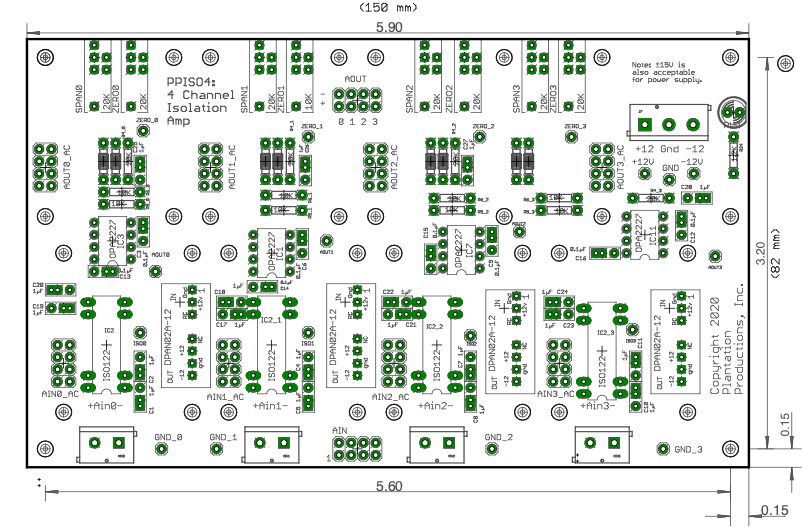
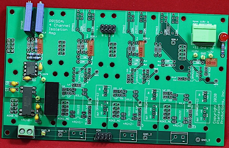
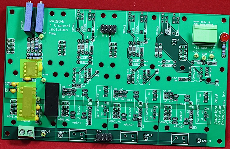
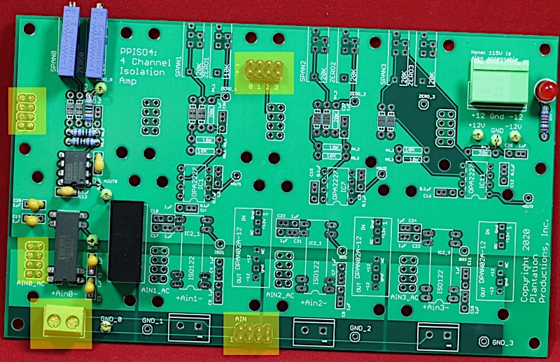
PPISO4
4-Channel Isolation Amplfier
High-resolution image
The PPISO4 board is a 4-channel analog isolation amplifier board. Each channel accepts an input voltage in the range ±10V. This is run through an isolation amplifier and feed into an amplifier circuit to allow adjusting the gain (span) and offset (zero) of the signal. The output is a single-ended voltage also in the range ±10V.
Note: The PPISO4 is an updated design replacing the older PPAC4 board. The PPAC4 board should not be used in modern designs. For more information about the PPAC4 board, follow this link.
The PPISO4 has the following features:
- Open Source/Open Hardware design (Creative Commons 4.0 license).
- Stable, low-drift design.
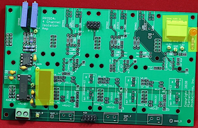
- ±12V power supply (can also run off ±15V).
- LED indicates when power is applied.
- 4 single-ended analog inputs supporting ±10V inputs (standard configuration)
- 4 single-ended outputs, supporting ±10V outputs (standard configuration).
- Electrical isolation (isolation amplifiers) on each input channel isolating all inputs from each other and from the DAQ system
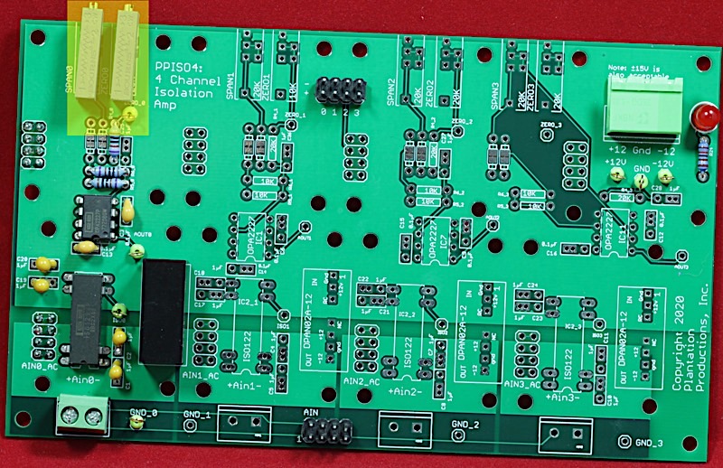
- Span and zero pots for all four analog channels allowing the adjustment of gain and offset (respectively).
- Minimum 1kHz bandwidth (note: DAQ system standard firmware scans analog inputs at a 40 Hz rate, so this is 25 times faster than needed by the DAQ firmware). Optional filter capacitor can reduce this to eliminate noise in an noisy environment.
- Optional DIN rail brackets allow installation on 35mm DIN rails.
- DIN rail brackets are available in .STL format for 3D-printing.
- Daughterboard support for input and output analog conditioning, including: differential input, 4-20mA input, differential output and 4-20mA output.
Bill of Materials (BOM) for the PPISO4 board
Channel-independent materials:
- (1) 5mm LED
- (1) 1.2 kΩ 1/4-watt 1% resistor
- (1) PPAC4 PCB
- (2) 8-pin (2x4) male headers
- (1) 3-pin screw terminal (5mm/0.2" centers)
- Optional: (3) test pins
- Optional: one set of horizontal 35mm DIN rail mounts for DAQ boards
- Optional: vertical 35mm DIN rail mount for PPISO4 board
Parts for each channel (four total channels):
- (1) 2-pin screw terminal (5mm/0.2" centers)
- (1) DPAN02A-12 (or DPAN02A-15) regulated isolation power supply
- (1) ISO122 isolation amplifier
- (1) OPA2227 dual opamp
- (2) 8-pin (2x4) male headers
- (2) 10kΩ 0.1% 15 PPM/C resistors
- (1) 20kΩ 0.1% 15 PPM/C resistors
- (2) 10 kΩ (or 20kΩ) 10% 50 PPM/C PCB trim pots
- (2) 0.1µF decoupling capacitors
- (4) 1µF tantalum decoupling capacitors
- Optional: (4) test pins
- Optional: (2) 5kΩ 0.1% resistors
- Optional: (3) test pins
PCB Availablity
Note: If you only want a few PPISO4 PCBs, contact Plantation Productions (randy@plantation-productions.com) to see if there are any in stock. Bare boards are $25 each plus shipping; fully assembled and tested boards are $750 each. If you need more than a couple PCBs and you're not in a huge hurry, it costs about $150 plus shipping (plus about 4-6 weeks) to have a set of 10 manufactured and shipped to you from China. I use Seeed Studio Fusion PCD service (https://www.seeedstudio.com/fusion.html). The PPISO4 PCBs are four-layer boards. Here are the files:
| Description | Link |
|---|---|
| Gerber files for PCB (provide these files to Seeed Studio or your personal PCB manufacturer) | PPISO4 Gerber Files for PCB |
| Eagle schematic capture and PCB layout files. Use these if you want to modify or enhance the EtherPort HCDOUT design, or re-layout the PCB using Eagle | PPISO4 Eagle files (Schematic and board layout) |
| On-line schematic (PDF format) | |
| PP Standard DIN rails (STL format for 3D printer) | PP Standard DIN Rail Brackets 3D printer files |
| Adjustable DIN rail bracket (STL format for 3D printer) | Adjustable DIN Rail Bracket 3D printer file |
Vertical DIN rail bracket (STL format for 3D printer) |
PPISO4 Vertical DIN Rail Bracket |
Vertical DIN Rail
Revision History
Rev 1:
Changed name to PPISO4 (from PPAC4 and PPACDO4).
Complete redesign for better stability.
Rev 2:
Switched input pins on opamps.
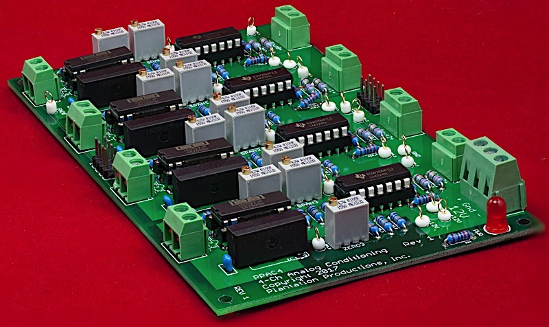
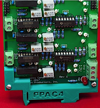
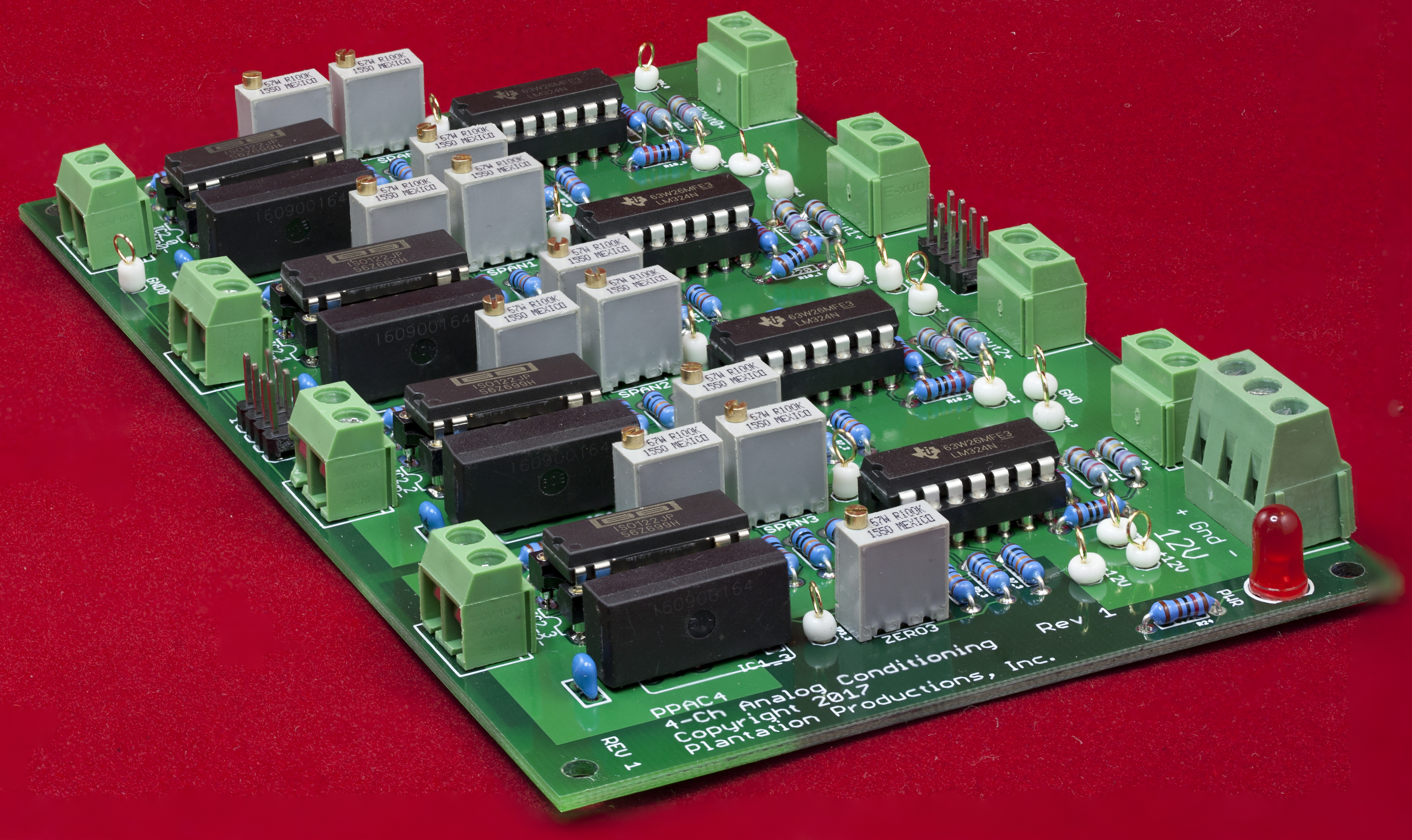
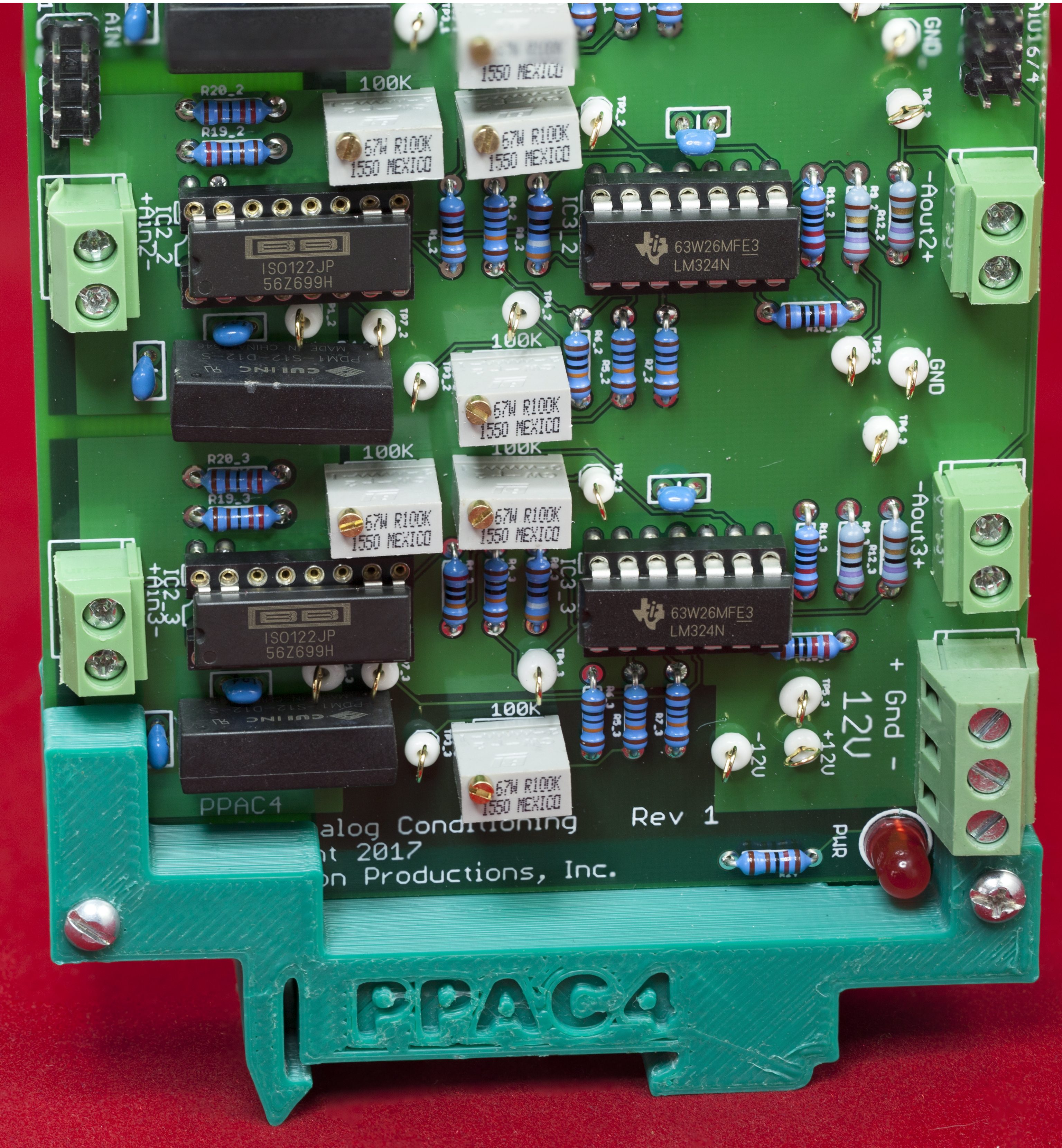
PPAC4 Board Layout
PPISO4 Daughter Boards
The original PPAC4 board (on which the PPISO4's design was based) accepted a single-ended input and produced a differential output. You could use a PPAC420 board in series with the PPAC4 to convert a differential input to a single-ended output and use that as an input to the PPAC4 to provide a 4-20mA input.
The PPISO4 board uses a different technique to handle 4-20mA and differential voltage I/O. The PPISO board supports single-channel "daughter boards" that attached to each channel. With no daughter boards attached (the standard configuration), a channel accepts a single-ended input voltage (in the range ±10V) and produces a single-ended output voltage (also in the range ±10V).
An input daughter board (connected to the 2x4 headers marked AINn_AC, where n is the channel number in the range 0 to 3) can accept a different analog signal and convert it to a single-ended voltage (somewhere in the range -10V to +10V). There are currently two different input daughter boards available:
- PPDiffIn- Converts a differential input in the range ±10V to a single-ended voltage in the range -5V to +5V (the gain of 0.5/-3dB can be restored back to 1/0dB by setting the gain on the PPISO channel to 2/6dB).
- PP420In- Converts a 0-20mA signal to a single-ended voltage in the range -1.25V to +5V (4-20mA becomes 0 to 5V).
Of course, the amplifiers on the PPISO4 board can convert these input values to any voltage in the range -10V to +10V by adjusting the SPAN and ZERO pots.
An output daughter board (connected to the 2x4 headers marked AOUTn_AC, where n is the channel number in the range 0 to 3) takes the single-ended output voltage from the PPISO4 and converts it to some other form. There are currently three different output daughter boards available:
- PPDiffOut- Converts the single-ended output to a differential output (two possible forms, one with a differential signal around 0V, one with a differential signal around a specified reference voltage).
- PP420Out- Converts the single-ended output to a 4-20mA current loop output.
- PPIsoOut- Converts the single-ended output to an isolated output (typically not used with the PPISO4 board, as the PPISO4 board already isolates the input from the output; this could, however, be used to further isolate the output from the PPISO4 circuitry, itself).
The use of the daughter boards allows you to configure the PPISO as follows:
| Inputs | Outputs | |||
|---|---|---|---|---|
Single-ended |
Single-ended -10V to +10V |
Differential (std in, PPIsoOut ) |
4-20 mA (std in, PP420Out) |
Isolated single-ended output -10V to +10V (std in, PPIsoOut) |
Differential |
Single-ended -10V to +10V (PPDiffIn, std out ) |
Differential (PPDiffIn, PPDiffOut) |
4-20 mA (PPDiffIn, PP420Out) |
Isolated single-ended output -10V to +10V (PPDiffIn, PPIsoOut) |
4-20mA |
Single-ended -10V to +10V (PP420In, std out) |
Differential (PP420In, PPDiffOut) |
4-20 mA (PP420In, PP420Out) |
Isolated single-ended output -10V to +10V (PP420In, PPIsoOut) |
Here's a picture of the PPISO4 with a PPDiffOut board installed on channel 0:
See the "Build a PPISO4 Board" section for more information on using daughter boards with the PPISO4.
Connections
The PPISO4 provides four 2-pin screw terminals for input connections (AIN0, AIN1, AIN2, and AIN3). There is also a 2x4 (8-pin) header which duplicates the input signals. The 2x8 header has the following connections:
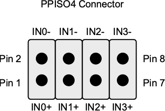
With the standard configuration, you would connect the input signal to the IN0+ (IN1+, etc., hereafter INn+) pin and the input ground to the IN0- (IN1-, etc., hereafter INn-) pin. For differential inputs (when using a differential input daughter board), you'd connect the differential (+) input to the INn+ pin and the differential (-) pin to the INn- pin. For 4-20mA inputs (using the 4-20mA input board), you'd connect the (+) current input to the INn+ pin and the (-) current input pin to the INn- pin.
Note that the input pins are completely isolated from the reset of the circuit (beyond the ISO122 IC). If you want to measure the voltage or current on the input pins, there is a special test pin labeled "Gnd_n" (where n is the channel number). This test pin is attached to the ground pin on the isolation power supply (on the input side). You can measure voltages on the input side relative to this test pin.
Note that the INn- signals are not common with respect to one another. All the input signals are isolated from one another (as well as from the rest of the PPISO4 circuitry). This is true even in the standard PPISO4 configuration.
The AOUT connector (2x4 header) has the same pinouts as the input header (except, of course, the signals are output signals rather than input signals. Note, however, that in the standard configuration (no daughterboard), the OUTn- signals are all common and connected to the main ground signal. If an output daughter board is installed on a given channel, then that channel's OUTn- signal(as well as the OUTn+ signal) is determined by the particular daughter board.
The AOUTn_AC connector on the PPISO4 (that mates with an output daughter board) has the following pinout:
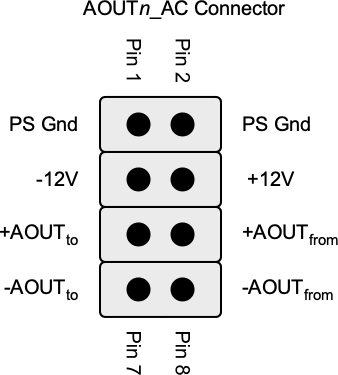
The PSGnd pins connect to the power supply ground on the PPISO4 board (the main power supply, coming from the three-pin connector). The -12V and +12V pins also come from the main power supply. Although they are labeled ±12V, keep in mind that the PPISO4 board can also be powered by ±15V, so it is possible that ±15V appear on these pins (all daughter boards currently available for the PPISO4 accept ±12V or ±15V on the power supply pins). Circuitry on the daughter board can obtain power from these pins (note that these are not isolated power supply pins, if the daughter board requires isolated power, it must use its own isolation power supply, fed from these pins, to produce isolated power).
The +AOUTto pin is the singled-ended signal from the PPISO board to the daughter board. The +AOUTfrom pin is the +AOUT signal from the daughter board back to the PPISO4 board (which the PPISO4 board routes directly to the +AOUTn pin on the output connector).
The -AOUTto pin is the single-ended (-) signal from the PPISO4. On the PPISO4, this is always the same as PSGnd (on different boards, this might not be connected to ground). The -AOUTfrom signal is the signal from the daughter board back to the PPISO4, which the PPISO4 routes directly to the -AOUTn pin on the output connector. Note that this may or may not be connected to PSGnd (the PPIsoOut daughter board, for example, produces an isolated -AOUTfrom signal).
In the PPISO4 standard configuration (single-ended signal in and single-ended signal out) with no daughter boards installed, +AOUTto must be connected directly to +AOUTfrom and -AOUTto must be connected directly to -AOUTfrom. This is usually accomplished by soldering a jumper wire between the two holes on the PPISO4 circuit board (see "Build a PPISO4 Board" for more details). In the standard configuration, the PSGnd, +12V, and -12V should be left unconnected to anything.
The AINn_AC connector on the PPISO4 (that mates with an output daughter board) has the following pinout:
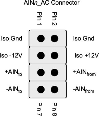
The IsoGnd pins connect to the ground PPISO4's isolation power supply for the specific channel. They do not connect to the ground on the main power supply. Likewise, the Iso-12V and Iso+12V pins connect to the ±12V outputs on the channel's isolation power supply. Although they are labeled ±12V, keep in mind that the PPISO4 board can also be powered by ±15V (with ±15V isolation power supplies), so it is possible that ±15V appear on these pins (all daughter boards currently available for the PPISO4 accept ±12V or ±15V on the power supply pins). Circuitry on the input board can obtain power from these pins, but keep in mind that the isolation power supplies on the PPISO don't put out that much power (all existing daughter boards work fine).
The +AINto pin is the signal from the PPISO board to the daughter board. This signal comes directly from the +AINn input connector. The type of analog signal appearing on the input is defined by the daughter board itself (it could be a single-ended input, a differential input, or a 4-20mA current loop input). Likewise, the -AINto is the other side of the signal directly from the -AINn input connector; this signal is not tied to any ground or other signal on the PPISO4 board.
The +AOUTfrom signal is the signal from the daughter board back to the PPISO4. This will be a single-ended signal (relative to -AINfrom). The -AINfrom signal is the ground reference for the signal from the daughter board; it is connected to the IsoGnd signal (from the isolation power supply).
In the PPISO4 standard configuration (single-ended signal in and single-ended signal out) with no daughter boards installed, +AINto must be connected directly to +AINfrom and -AINto must be connected directly to -AINfrom. This is usually accomplished by soldering a jumper wire between the two holes on the PPISO4 circuit board (see "Build a PPISO4 Board" for more details). In the standard configuration, the IsoGnd, Iso+12V, and Iso-12V should be left unconnected.
Test Pins
Each channel on the PPISO4 has four test pins:
- Gnd_n (n is the channel number): This is the isolated ground for the input. Measure input voltages on the isolation side (of the ISO122 isolation amplifier) relative to this ground, not the main power supply ground.
- ISOn (n is the channel number): This is the output from the ISO122 isolation amplifier. Measure this voltage relative to the main power supply ground.
- AOUTn (n is the channel number): This is the output from the SPAN (gain)/ZERO (offset) amplifier stages. This is the single-ended output from the PPISO4 board, before the signal is fed to the daughter board (if one is installed).
- Zero_n (n is the channel number): This is the voltage output from the ZERO (offset) pot. Note that the offset value is fed through an inverting amplifier, so the voltage you measure on this pin will actually be inverted compared to the output the PPISO4 produces. For example, if you measure +2.1V on this point, the circuit is actually subtracting 2.1V (adding -2.1V) to the signal.
In addition to the 16 test pins (four per channel), there are three additional pins connected to the power supply signals (Gnd, +12V, and -12V).
Building a PPISO4 Board
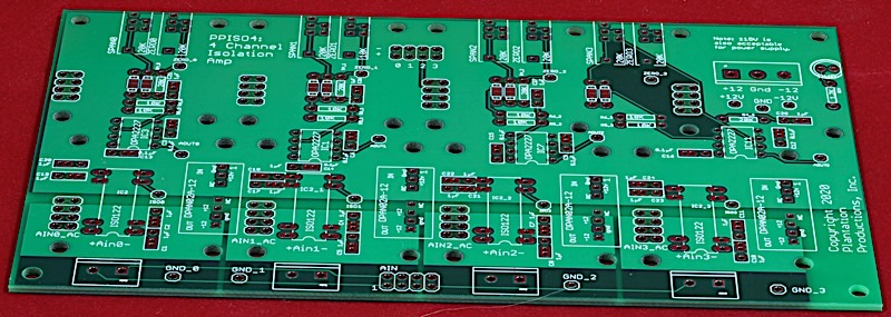
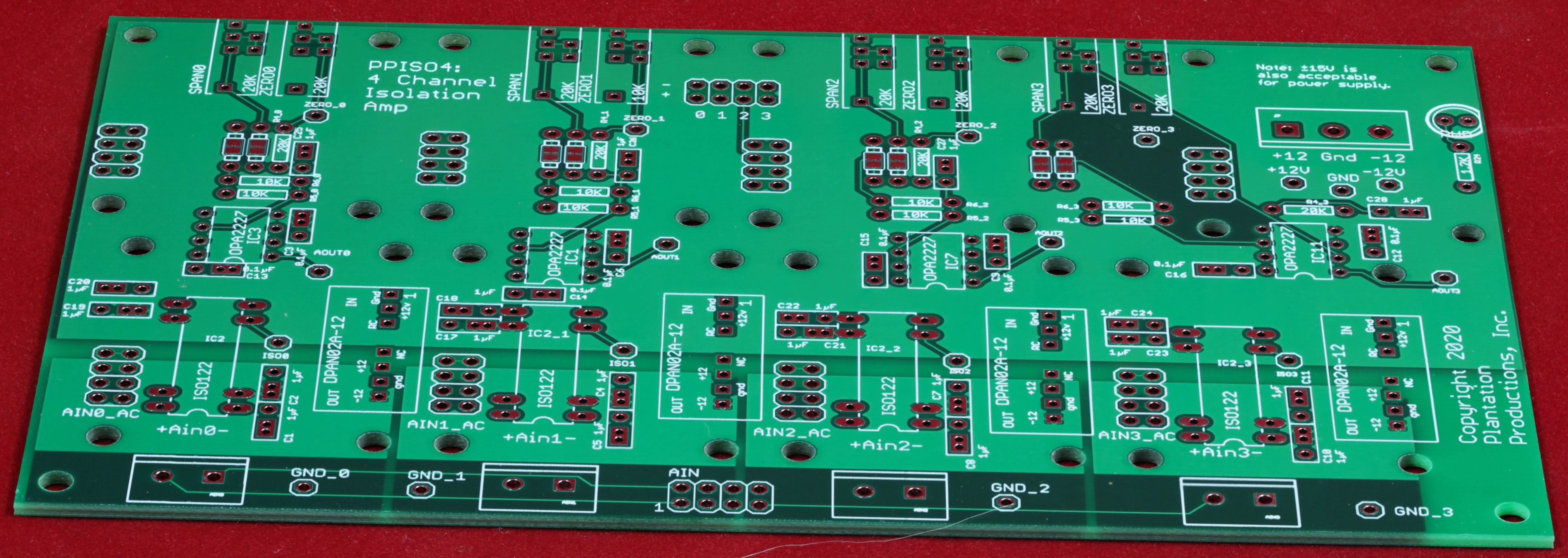
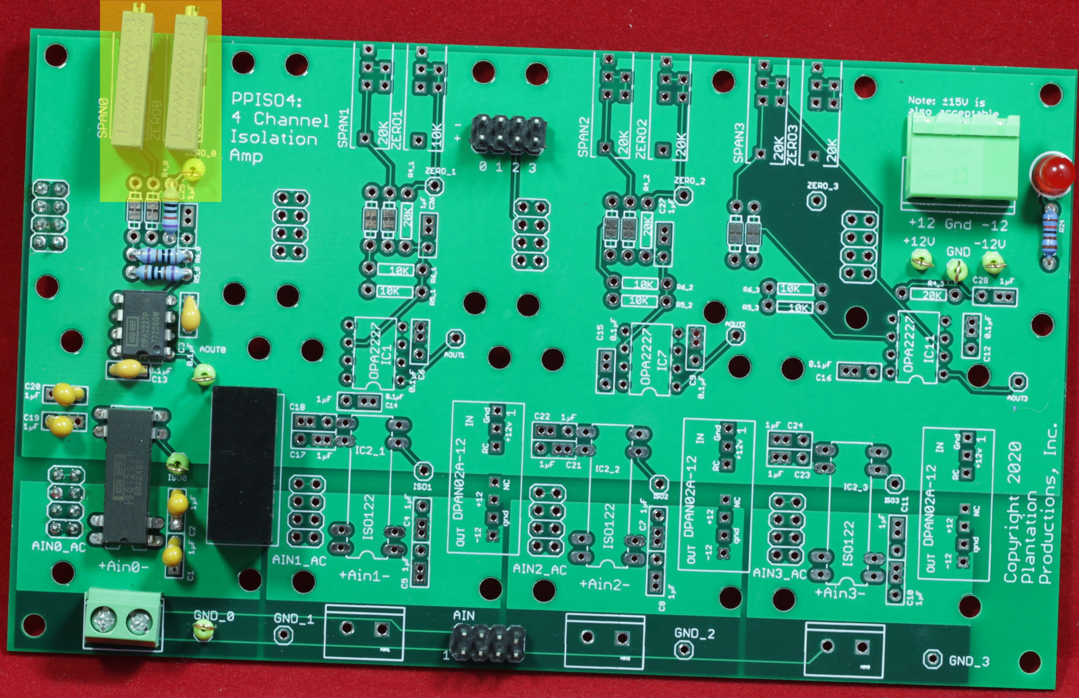
Here's the bare PPISO4 PCB (printed circuit board):
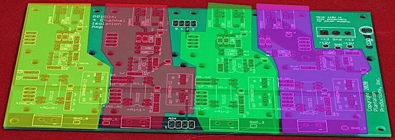
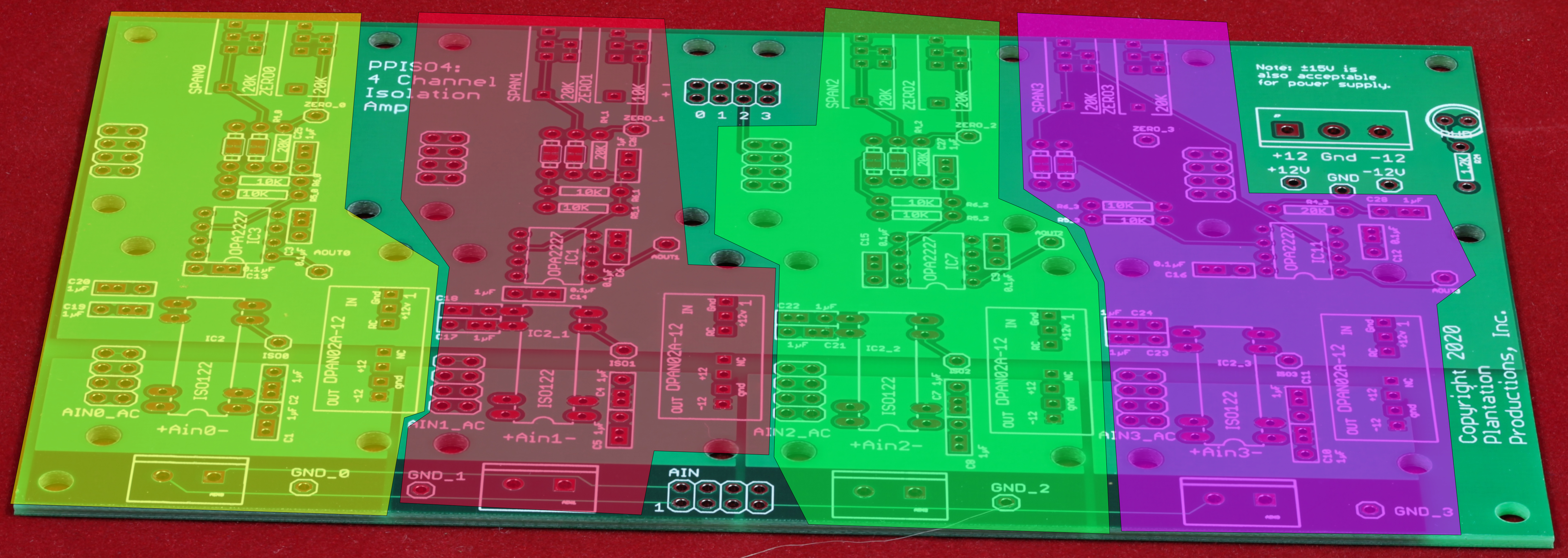
The PPISO4 contains four independent channels:
Although the usual build process is to build a board from "the bottom up," I generally recommend building the PPISO4 board one channel at a time. These instructions describe the construction of Channel 0 on the PPISO4 board; the instructions for the other three channels are almost identical (some parts have moved around, but otherwise construction is identical).
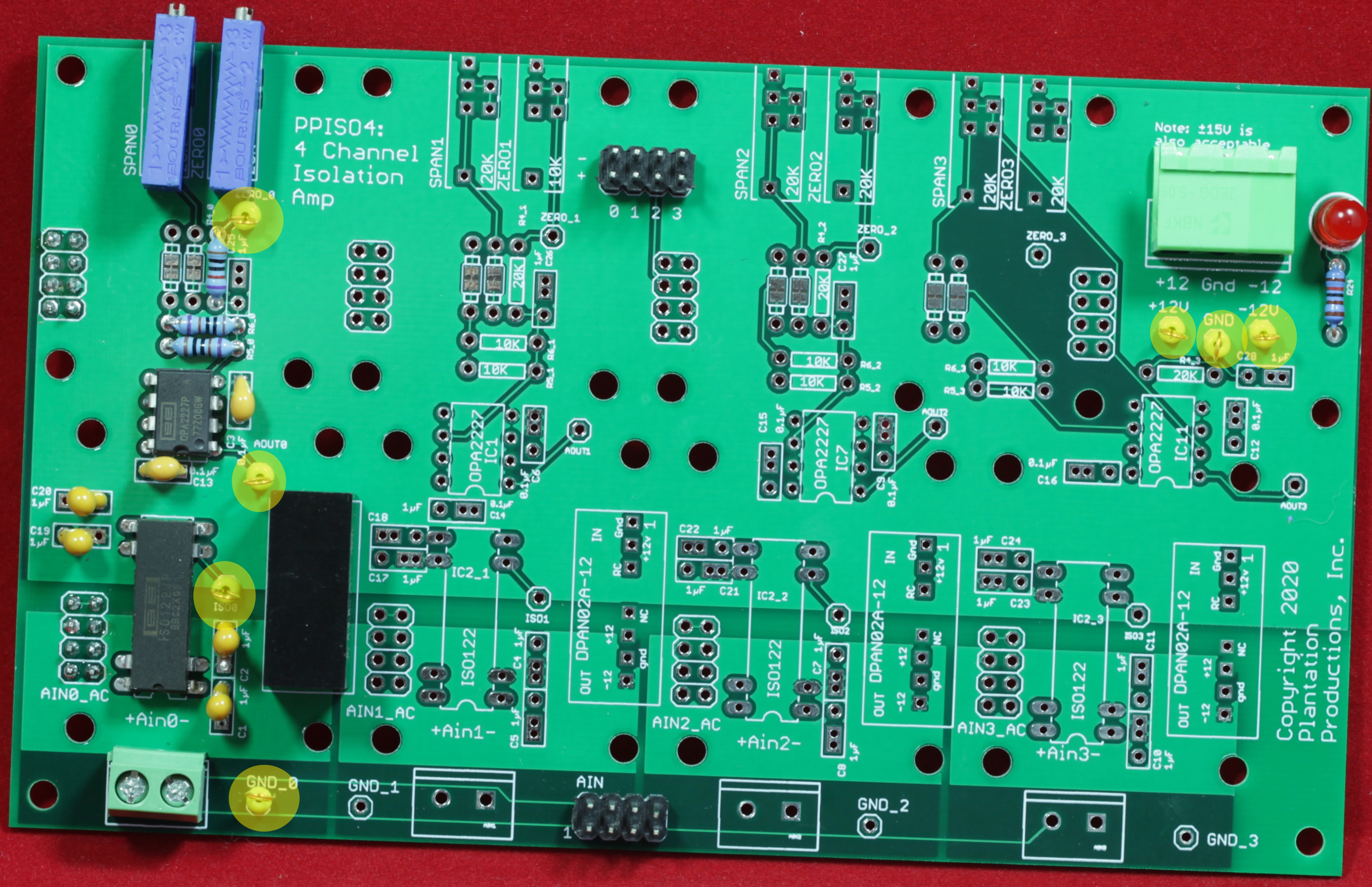
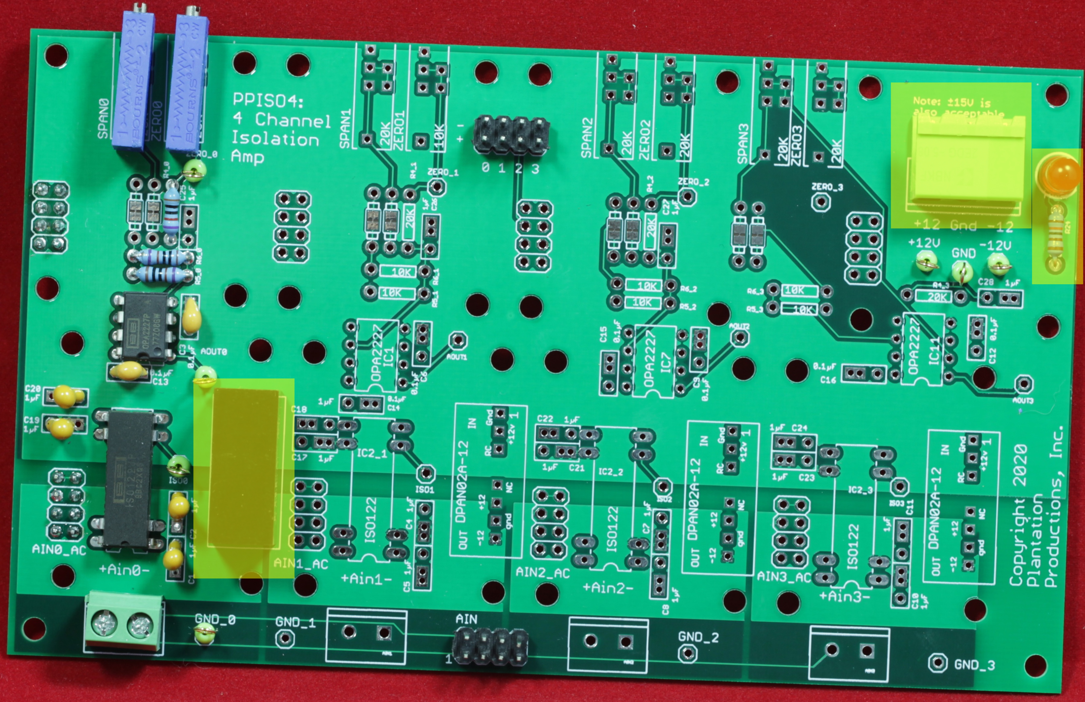
- The usual build process is to build a board from "the bottom up." This means to first install those items closest to the PCB and work you way up to larger objects on the PCB. The smallest items on the PPISO4 board at the test pins, so solder them onto the board first:
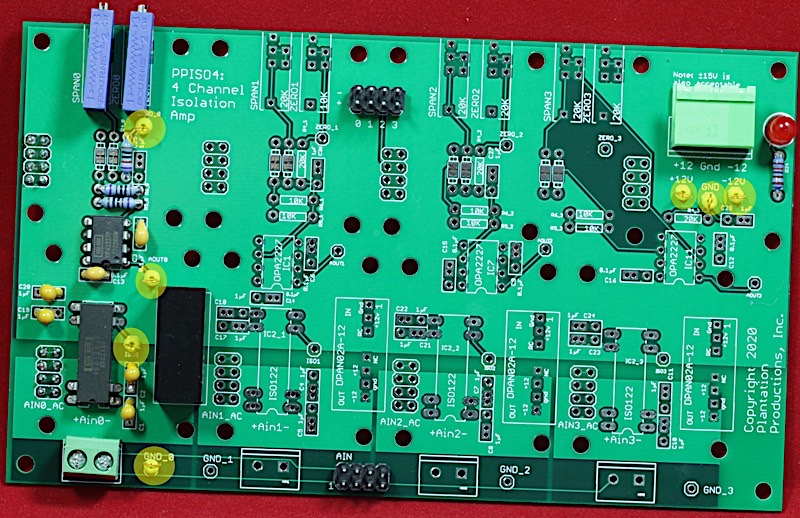
High resolution image
While installing the four test pins for Channel 0, you may as well install the three test pins by the power supply connector (as they will be handy when testing Channel 0).
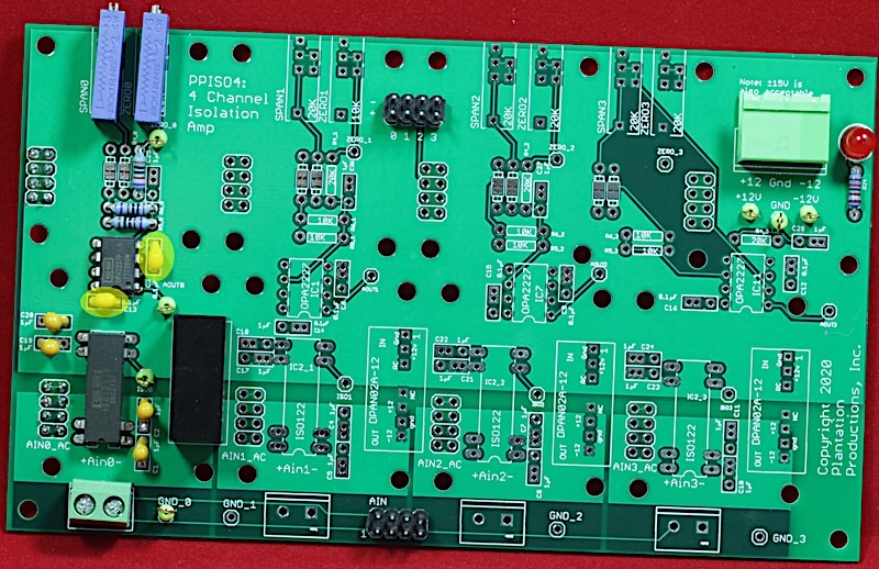
- Next, solder on the two 0.1µF bypass capacistors:
High resolution image
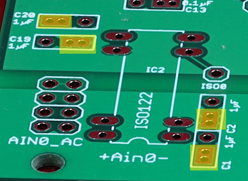
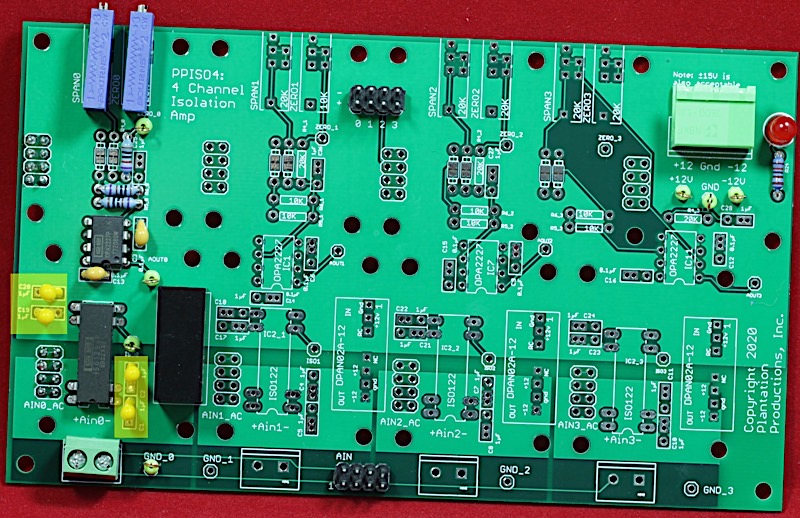
- Next, install the four 1µF Tantalum bypass capacitors. Note that tantalum capacitors are polarized. The short pin (-) must go in the pad with two holes on it:
High resolution image
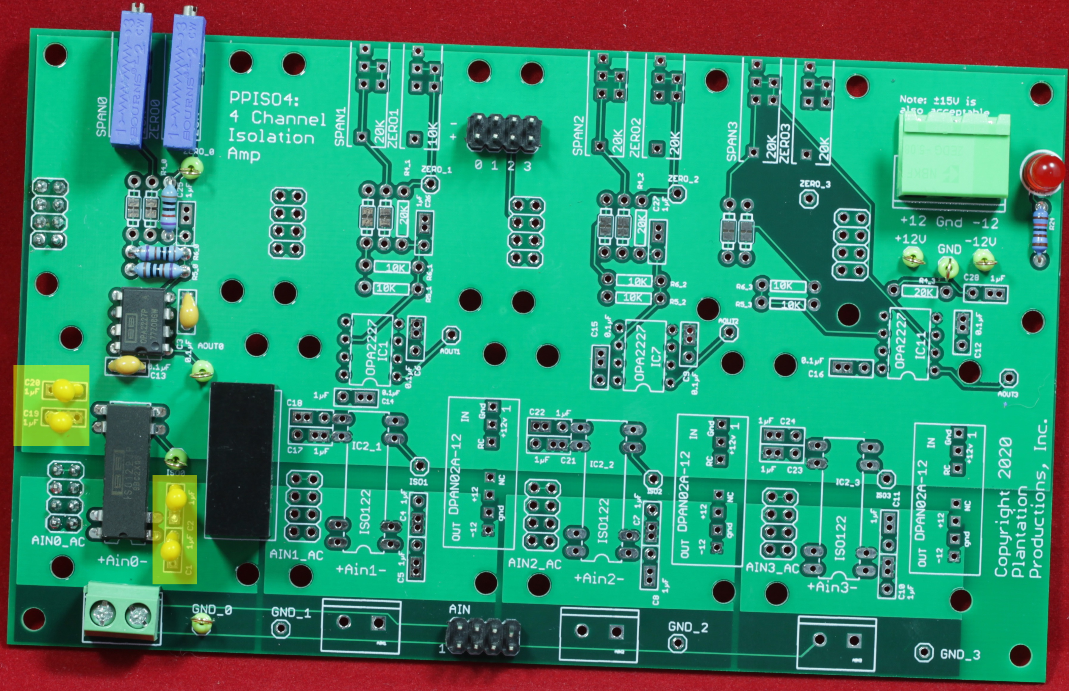
- The next step is optional: install a 1µF filter capacitor. If you have a noisy environment, this will filter out all signals whose frequency is above a couple hundred Hertz. Most data acquisition systems scan their ADCs at a fairly low frequency (like 10-20Hz). Putting in this capacitor can reduce errors in a noisy system. As a general rule, I don't install this capacitor unless it's actually needed (experimentally determined), so I didn't install one on the example board; I generally recommend waiting on the installation of this part. However, if you know you want to filter out higher frequency noise, you can install this during initial construction. I have pointed out the position of this capacitor in all four channels in the following picture. This are also 1µF tantalum capacitors–watch the polarity! Again, the pads with the two holes are the negative terminals.
High resolution image
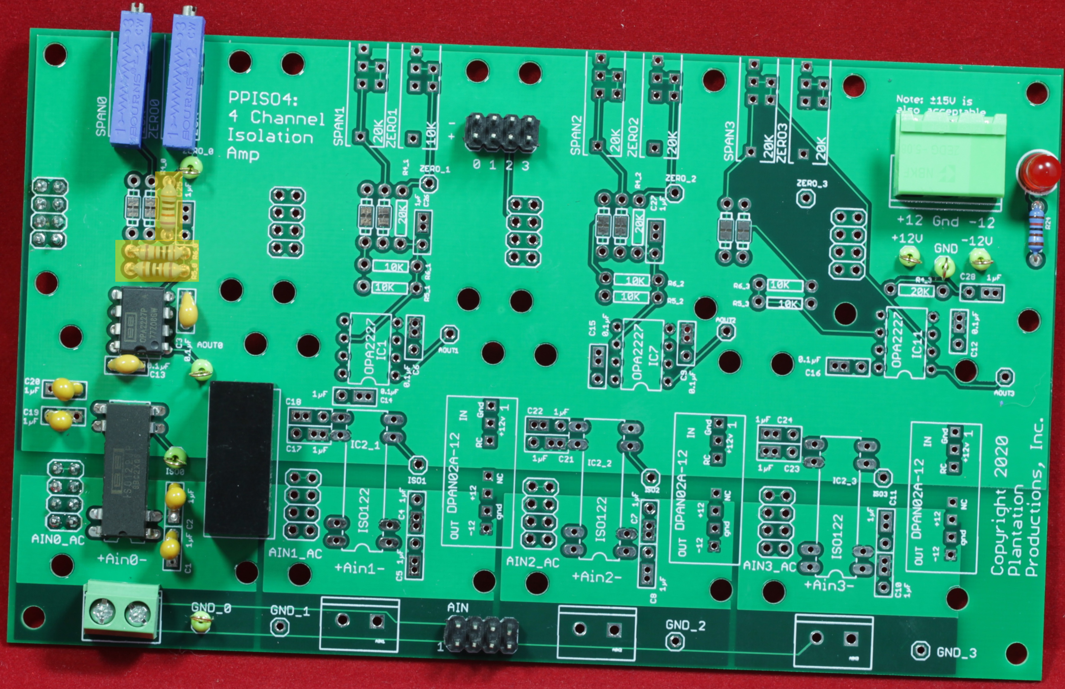
- The next thing to install are the resistors. There are three resistors that must be installed for each channel–nominally two 10kΩ and one 20kΩ resistors; however, see the Hardware Design Description for details on the actual values of these resistors; these values are not absolutely fixed, you can choose different values based on your particular situation.
High resolution image
- There are two optional resistors you can install on this board. See the Hardware Design Description for a description of the purpose of these resistors. There are currently a couple of solder pads with a trace between them. You must cut these traces if you want to install these resistors. The nominal value for these resistors is 5kΩ; see the HDD for more information about their values and specifications.
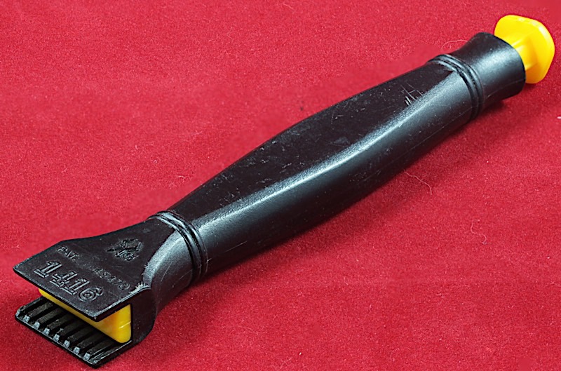
- The next step is to insert the ICs (the ISO122 and OPA2227).
When inserting ICs, you will notice that the pins on the ICs are actually slanted outward and will not directly fit in the holes on the board (or in holes on the sockets, for that matter). If you have an IC inserter tool, it will automatically bend the pins to the appropriate position prior to insertion. If you don’t have such a tool available, just hold an IC with your fingertips with one row of pins against your workbench or desk and manually bend the pins until they are perpendicular to the body of the IC. Repeat for the pins on the other side of the IC.
Note: avoid the temptation to use sockets for the ICs. Yes, the ISO122 and OPA2227 are not cheap (around $8-$10 each). However, by socketing this ICs you destroy their precision by introducing thermal inaccuracies and noise. If you're going to socket these ICs, you'd be better off using "jellybean" opamps and saving a lot of money (though the accuracy of the circuit will suffer dramatically, see the HDD for details).
IC Insertion Tool:
High resolution image
Board with ICs soldered directly to the PCB (this is the recommended assembly version):
High resolution image
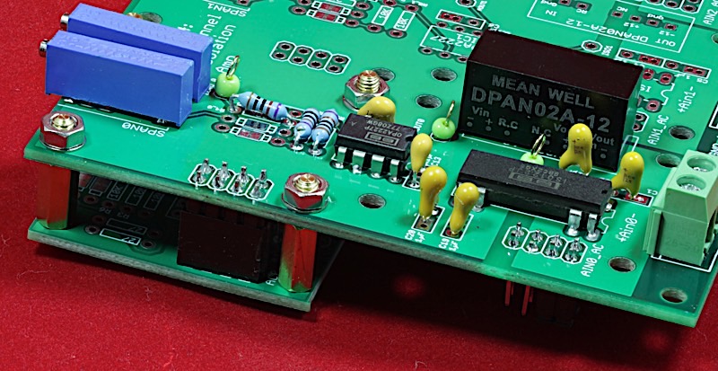
- Next, install the two potentiometers. The schematic claims these are 20kΩ pots. However, I usually install 10kΩ units because they're much less expensive (at least from my sources). See the Hardware Design Description for a discussion of pot and resistor values (as well as their specs and prices; these are not cheap parts).
High resolution image
- For the next step, solder the DPAN02A-12 isolation power supply, LED, 1.2kΩ resistor, and power connector onto the PCB.
High resolution image
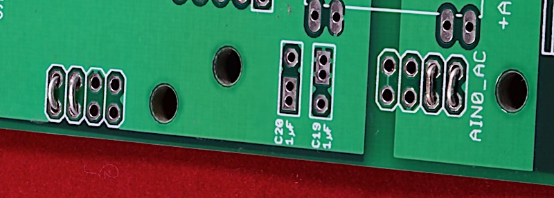
- The next step is to solder on the headers and the screw terminals. There are two sets of 2x4 (8-pin) headers for Channel 0. These are for the input and output daughter boards. Normally, the daughter boards are installed on the back of the PPISO4, providing easy access to connectors and test pins on the top of the board. For example, the following picture shows a PPDiffOut board installed on the back of a PPISO4 board:
High resolution image
As you can see in this picture, the 2x4 headers are installed with the long pins facing down on the board. In theory, you could also install the headers with the pins up (installing the daughter boards on the top of the PPISO4). Of course, you'll have to solder the female header on the daughter board on its bottom rather than on the top (where it normally goes). You might also need longer pins on the daughter board's female header so the daughter board clears the isolation power supply and trim pots. Unless you have some good reason for doing so, it's probably best to install the daughter boards on the bottom of the PPISO4.
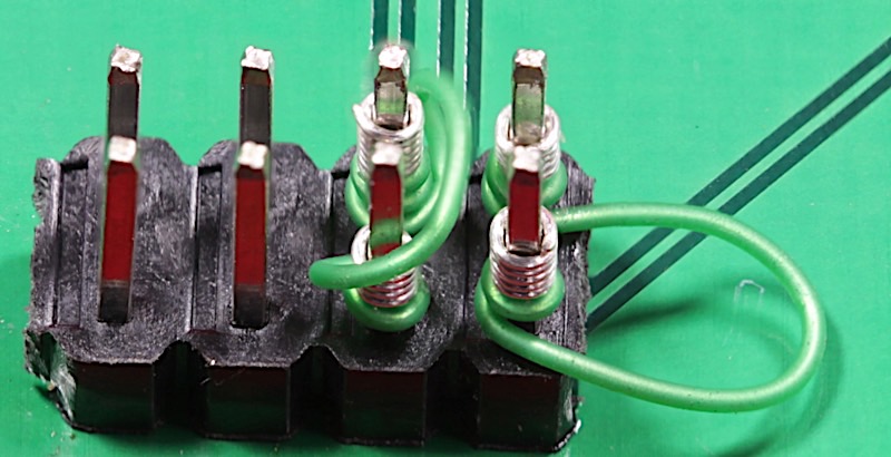
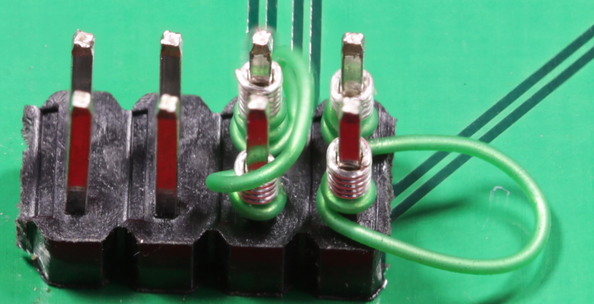
Note that installing the daughter board headers is actually an optional step. If you plan on using the PPISO board in the standard configuration (singled-ended inputs and outputs), then the best solution is to simply install two jumper wires in the headers as follows:
High resolution image
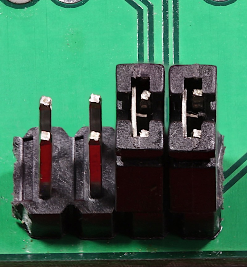
If you install headers and decide you want to operate the board in the standard configuration mode, the best solution is to put wire-wrap wire on the posts (and even touch them with a soldering iron and some solder to make an even better connection):
High resolution image
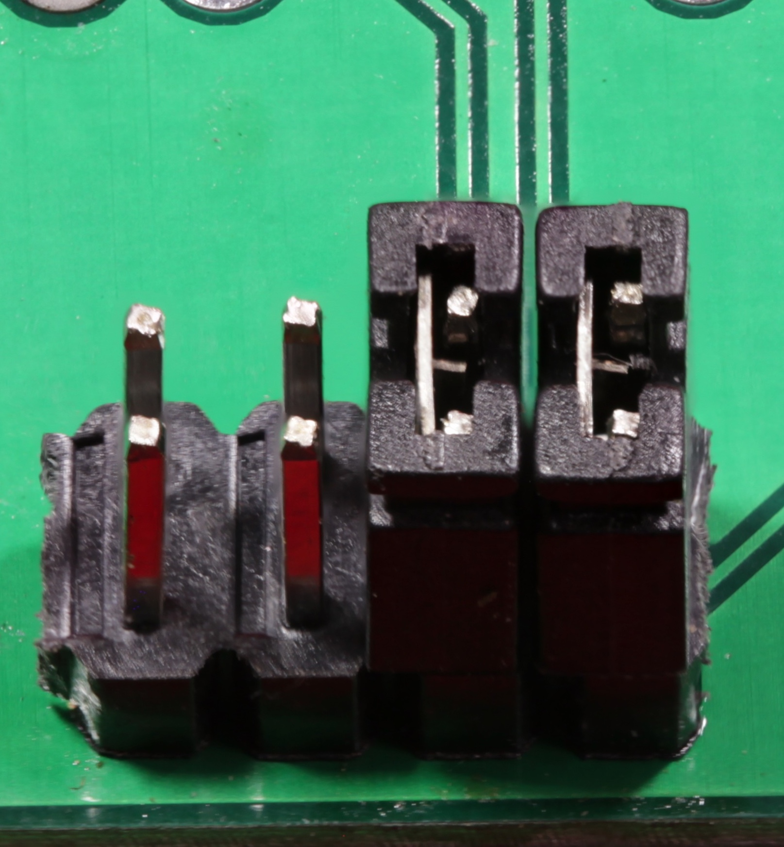
As a temporarly solution (during testing and calibration), you can stick a couple of jumpers on the pins. This, however, is not a good long-term solution. Jumpers have the same problems as sockets – they have lousy thermal characteristics and they're noisy:
High resolution image
While you are installing the two 2x8 headers for the daughter boards (assuming you install them), you may as well install the two 2x8 headers for the AOUT and AIN pins. Also, install the 2-pin screw terminal during this step:
High resolution image
- At this point, soldering is largely complete (assuming you’ve made no mistakes that will require some rework). Turn the board over and slowly, careful, visually inspect every solder joint. Well over 50% of the failures I’ve had were due to missing a solder connection. It’s worthwhile to visually inspect all the pins (yeah, I know, there are a lot of them) to verify you haven’t missed any.
- Now for the actual “smoke” test. With the ICs inserted, apply power and make sure the LED still lights up (no flickering!) and nothing gets overly hot (or worse, smokes and catches on fire! Yes, this has happened to me in the past).
- Assuming you want to build all four channels, repeat these steps for the other three channels (minus, of course, installing the parts that are common to all channels).
Testing and Calibrating the PPAC4 Board
The PPISO4 board contains two calibration pots for each channel to set the ZERO (offset) and SPAN (gain) values.
The ZERO pot is useful because the ISO122 isolation amplifier always adds a small voltage offset to the output of the amplifier (that is, if you put in exactly 0V as input to the ISO122 you'll probably not get exactly 0V as the output from the amp -- the ISO122 can add a small negative or positive voltage offset to the input voltage). Also, it's unlike the plus and minus legs of the ±12V power supply are exactly equal in magnitude, so the ZERO pot can help offset for differences there as well as inexact resistor values in the opamp circuits.
The SPAN pot adjusts the overall gain of the opamp circuit (note that a dual opamp circuit follows the isolation amplifier; the isolation amplifier has a gain of 1 which is not adjustable). The PPISO4 board accepts an input voltage that can range from -10V to +10V input and it can produce an output voltage also in the range -10V to +10V. This does not imply that the output voltage must exactly match the input voltage (i.e., a gain of one). You could, for example, have 0 to 5V input voltage that produces a -10V to +10V output (very typical of processing the output of a digital-to-analog converter). As another example, you could take a -10V to +10V input from the field and produce an output voltage in the range 0 to 3.3V, for use as input to an analog-to-digital converter on a 3.3V microprocessor.
Calibrating the PPISO4 consists of iterating the following steps for ±10V operation (input and output, with a gain of 1):
- First, begin by setting the zero voltage (measured at test pin Zero_n and the main power supply Gnd) to around 0V by adjusting the ZEROn pot.
- Next, supply an input voltage of -10V to the channel and measure the amplifier section output voltage on test pin AOUT_n (where n is the channel number, 0 to 3).
- Adjust the ZERO pot until you read a voltage of -10V on test pin Aout_n.
(If you don't have a power supply that produces postive and negative voltages, just swap the plus and minus leads on the power supply to get negative voltages.)
- Supply an input voltage of +10.00V to the channel you're calibrating and measure the amplifier section output voltage on test pin Aout_n.
- Adjust the SPAN pot until you read a voltage of +10.00V on Aout_n. Note: if the initial reading is greater than +10.00V, reduce it to a value less than +10.00V and then slowly adjust the output back up to +10.00V.
- Repeat steps 2 through 6 until the ZERO point and SPAN are reasonably close (note that adjusting one pot will affect the other pot's results, so you will have to iterate over this process several times.
Note that because of inaccuracies in the components, the power supplies, temperature, humidity, noise, etc., it is unlikely that you will exactly -10.00V, and +10.00V.
The only problem with the calibration steps above is that they use a base voltage of -10.00V. This is fine if you want the PPISO4 to respond to the whole range with the accuracy (across the whole range) as good as possible. The only problem with calibration is that if you put in 0.00V, you may be slightly off on the output. This generally occurs if the legs of the power supply (-12V and +12V) aren't exactly equal other than their sign. For example, if the -12V leg is actually -12.05 and the positive leg is actually +12.2V, calibrating the system to -10V and +10V may wind up with 0.00V (input) actually registering something like 0.1V. In many applications, a 0.00V input should produce an output as close to 0.00V as possible (even if it means that the -10V or +10V signals are off a small amount). If you're application requires a 0V input to produce a 0V output, then modify the calibration scheme as follows:
- First, begin by setting the zero voltage (measured at test pin Zero_n and the main power supply Gnd) to around 0V by adjusting the ZEROn pot.
- Next, supply an input voltage of 0.000V to the channel and measure the amplifier section output voltage on test pin AOUT_n (where n is the channel number, 0 to 3).
- Adjust the ZERO pot until you read a voltage of 0.000V on test pin Aout_n (or as close as you can get to it).
- Supply an input voltage of +10.00V to the channel you're calibrating and measure the amplifier section output voltage on test pin Aout_n.
- Adjust the SPAN pot until you read a voltage of +10.00V on Aout_n. Note: if the initial reading is greater than +10.00V, reduce it to a value less than +10.00V and then slowly adjust the output back up to +10.00V.
- Supply an input voltage of -10.00V to the channel you're calibrating and measure the amplifier section output voltage on test pin Aout_n.
- Whatever the difference is, split that in half and readjust the SPAN at +10.00V so that it's off half the error on the -10.00V side.
- Once again, supply an input voltage of -10.00V and verify that you've split the difference in half (repeat steps 4 through 8 until both sides are off by the same amount).
- Repeat steps 2 through 8 until the ZERO point and SPAN are reasonably close (note that adjusting one pot will affect the other pot's results, so you will have to iterate over this process several times.
This calibration process assumes a ±10V input and a ±10V single-ended output. If you're planning on installing daughter boards on the PPISO4, I recommend calibrating the PPISO (all four channels) in the standard configuration first. Then install the daughter boards and repeat the process. Obviously, based on the types of inputs and output you may need to supply or measure something other than voltage. A current source is helpful for the PP420In board; a current meter will be necessary when connecting a PP420Out board. For differential input and output, just treat the differential inputs as single-ended inputs during calibration.
Hardware Design Description
The PPISO4 is a major redesign of the PPAC4 board. The original PPAC4 accepted a single-ended input and produced a differential output compatible with the ADS1115 ADC convertor (found on the PPAIO-16/4 board). Although the PPAC4 could be hacked to work as an analog conditioner for other purposes, it really was specifically designed for use with the PPAIO-16/4. Problem number one.
Another problem with the PPAC4's design is that it was designed to use low-cost "jellybean" parts such as the LM324 quad opamp and low-cost resistors and potentiometers. The problem with such parts is that they have less than stellar thermal stability and the PPAC4 outputs tended to drift with temperature and other environmental issues. Problem number two.
A big problem with the PPAC4 design is that it used unregulated isolation power supplies. The voltage output from those devices tends to drift with temperature, also cause the outputs on the PPAC4 to drift.
Next, the PPAC4 required separate boards in series with it to handle things like 4-20mA input (or output) or differential inputs (the PPAC4 did provide differential outputs).
Finally, there are a few design tweaks to the PPAC4 that could result in less drift, less noise, a more stable output, and easier calibration. Some of these features were added to the PPAC4 to produce the PPACDO4 board. The PPACDO4 board was used in a piece of instrumentation and the limitations of the original PPAC4 design became apparent. As a result, the PPISO4 board was designed to replace the PPACDO4 (and PPAC4).
The main goal of the PPISO4 design was to produce a board that, once calibrated, would hold that calibration for a reasonable length of time (i.e., no more than a couple calibrations per year, at most). Fundamentally, this meant disposing with the jellybean parts (e.g., $0.50 for an LM324 opamp, $1.50 for a trim pot, and a few cents each for 1% resistors) and designing the PPISO4 using instrumentation-quality opamps and resistors. Instrumentation-quality opamps are 10x to 20x more expensive than jellybean opamps (e.g., OPA2227 dual opamps are about $6 each [qty 1] while LM324 quad opamps are about $0.37 each [qty 1] from Mouser Electronics). Whereas cheap 1% metal-film resistors are a couple cents each, precise, low TCR, resistors range from about 10x that amount ($0.25 each) to as much as $5.00 ([or more) depending on how precise you want them. Potentiometers are just as bad. Rather than $0.50 to $1.50 for a typical trim pot, quality pots (with nowhere near the precision or TCR rating of individual resistors) run anywhere from $15.00 to $50.00 for "just good enough." Really, really, good pots can actually cost hundreds of dollars each (too rich for this design!).
When choosing the parts of the PPISO4 design, reducing output drift (given a stable input) was one of the primary goals. For opamps, the primary features were:
- High CMRR value
- Low input bias current
- Low offset voltage
- Low noise
- Wide power supply range (at least ±18V to handle the ±12V or ±15V required by the PPISO4).
For resistors and pots, the main characteristic to consider was the thermal coefficient of resistance (TCR). This parameter determines how much the resistance will change as a function of temperature. Resistance precision was a secondary concern for individual resistors (not as much for potentiometers).
The TCR rating is especially important for combating drift. Consider the following opamp circuit in the PPAC4 design:
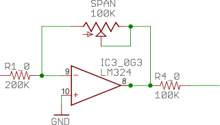
This is a very typical inverting opamp design. The gain is given by -Rfeedback/Rinput (-RSpan/R1_0). Adjusting the pot changes this ratio and, therefore, adjusts the opamp gain. In this particular schematic, the gain ranges from 0 (when RSpan = 0) to -0.5 (when RSpan = 100kΩ). The gain is negative because this is an inverting opamp.
Suppose the pot was set to 50kΩ and left there. As the system (and environment warms up), the resistors' values change. The TCR rating (typically given as PPM/C) defines how much the resistor changes with varying temperatures. Crappy (jellybean) resistors have TCR ratings in the high hundreds (even thousands). Assuming the two resistors (R1_0 and the SPAN pot) changed their resistance in an identical fashion with respect to temperature, this wouldn't be too big of a deal: it's the ratio of the resistance that is important, not the actual resistance values. If the two resistors' values changed (on a percentage basis) in lockstep with the temperature, the ratio would remain fairly constant and the gain wouldn't change that much.
Unfortunately, two different resistors aren't going to have the same exact TCR and, in fact, pots usually have far worse TCR ratings than individual resistors. Therefore, as the temperature changes, the two different resistors will change values at different rates. This will cause the ratio of the resistances to change and, therefore, the gain will change. This will cause the output voltage to drift even though the input voltage remains stable.
The first solution is to choose better resistors (ones with a low[er] TCR rating). For the most part, that's easy enough to do. All it takes is to throw some money at the problem. For example, in quantity one, Mouser Electronics lists a 10kΩ resistor with a TCR between 350 and 500 for around $0.10. Of course, go to Amazon and you can find 100 of them for around six bucks (though no TCR is given, assume it's bad). Indeed, if you buy 1,000 of them on Amazon, you can find carbon-film resistors for around $0.01 each.
Go to Mouser and search for 10kΩ, 15 PPM, 0.1% resistors. You'll find they cost about $0.51 each in quantity 1 ($0.274 each in qty 100). So spending 50 cents each (or a little more than a quarter each, if you buy them in 100 quantity), you'll get much better stability in the circuit.
Can we do better? Sure. How much money do you want to spend? Mouser lists a 10kΩ, 0.01%, 5 PPM/C resistor for only $13.06 (qty 1, qty 100 is $10.05). Do you want to spend over $117 dollars just for the resistors on your PPISO4 board? I didn't think so. Actually, there's a very pratical reason for not getting resistors that precise–the PCB has its own TCR rating which will be higher than 5 PPM/C. The weakest link in this case is the PCB, so there's really no reason for spending money on high-precision, low-TCR, resistors; the thermal drift from the other components on the board will completely swamp the accuracy of the resistors.
The other issue is the potentiometers on the PPISO4 board. Although you can get very low TCR, highly precise resistors (if you're willing to pay for them), pots are another issue altogether. Decent pots are 50 PPM/C at 10% accuracy. Such pots cost $13.00 and go way up depending on the resistance. You're also very limited in the resistances you can get; for example, you won't find a low-TCR pot at 100KΩ (at least, not without spending a huge fortune on the pot.
The PPISO specifies 20kΩ pots for the Span and Zero pots. As it turns out, Mouser has 20kΩ pots (50 PPM/C at 10%) but they cost more than 10kΩ parts. When used as voltage dividers, the resistance doesn't matter too much (as long as too much current doesn't flow through the whole pot). So I commonly swap out 10kΩ pots for the 20kΩ pots when building boards.
Here's the schematic for one amplifier section of the PPISO4:
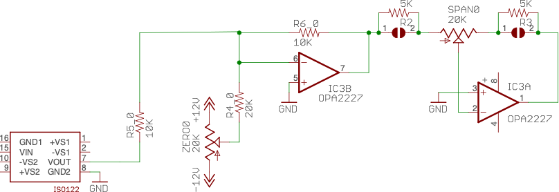
I'll discuss the second stage of the amplifier in a bit. For now, consider the first stage (opamp IC3B, R6_0, R4_0, R5_0, and the Zero0 pot). The input resistor is 10kΩ as is the feedback resistor. Therefore, this stage provides (roughly) unity gain for the input signal (well, -1 gain as it is an inverting amplifier). This is an inverting summing amplifier, adding the input voltage plus 1/2 the voltage coming out of the Zero0 pot (1/2 of this voltage because R4_0 is twice the resistance of R5_0). Because the Zero0 pot divides the voltage between -12V and +12V, this stage of the amplifier can add ±6V to the input signal.
Of course, R4_0 could also be a 10kΩ resistor. In that case, the Zero0 pot would be able to add ±12V to the input signal (though, technically, the PPISO4 circuit is rated for handling ±10V). However, in real-world situations, most voltage offsets added by a Zero pot are limited to plus or minus a couple of volts. So there really is no reason to allow the full scale ±12V to be added to the input voltage. Cutting the offset voltage in half has one desireable effect: you have to turn the pot twice as many turns to sum in the same voltage as you would if R4_0 had been 10kΩ. This means it's easier to "zero out" the circuit with a fair amount of precision.
If 20kΩ is good, why not go to 40kΩ and make the Zero0 pot even more precise? If you can guarantee you never need more than ±3V for the offset adjustment, this would make sense. However, some ADCs out there don't like negative voltages. So to convert a negative input voltage (say -5V to +5V) to a positive range, you might need to add more than 3V to the input. 20kΩ seemed like a good starting point for the design. However, you can replace this resistor with a larger (or smaller) value depending on your particular requirements.
As for the PPAC4 design, the R5_0/d R4_0 (input) and R6_0 (feedback) resistors determine the gain of this circuit based on their ratio. When the temperature changes the gain will vary if the resistors' ratio doesn't remain constant. Low TCR (e.g., 15 PPM/C) help prevent the gain from varying too much when the temperature changes.
Note that the resistors' precision (typically 0.1% for these resistors) means that the ratio will be very close to the calculated numbers. That is, ignoring the Zero0 pot sum value (assume it's 0V), the gain will be very close to unity (within the 0.1% tolerance of the resistors).
Pots are a different problem. First of all, the TCR values for pots are usually much higher than for discrete resistors (e.g., 50 PPM/C for the pots specified for the PPISO4, versus 15 PPM/C for the discrete resistors). Fortunately, the Zero0 pot is simply a voltage divider. It's value does not directly affect the gain of the opamp stage. Now the voltage divider could have issues if the resistance on one side of the pot's wiper changes with respect to the resistance on the other side of the wiper. However, as the pot is all one unit, the temperature is going to be relatively stable across the whole device and the whole device's resistance will change together. As a result, the effective TCR of the "two" resistors making up the voltage divider is very low (indeed, the wiper probably contributes more to the TCR variance than the actual pot material does).
Now consider the second stage of the amplifer in the circuit given above. This consists of two optional discrete resistors and a pot acting as a voltage divider. This is a big design change from the PPAC4. Look back at the PPAC4 amplifier circuit: The R1_0 and SPAN pot form a voltage divider (with one side of the divider having a fixed resistance and the other side having a variable resistance). As noted before, as the temperature changes, the resistances of the two halves of this voltage divider change by differing amounts, resulting in a gain that drifts with temperature.
Note look at the second stage of the PPISO4 circuit. The input and feedback resistors are both incorporated into the SPAN0 pot. That is, the left side of the pot (in the schematic diagram) is the input resistor and the portion of the pot to the right of the wiper is the feedback resistor. By combining the two resistors into a single pot, a fair amount of problems with thermal drift go away. Using a decent quality pot (50 PPM/C and 10% tolerance) produces a very stable design.
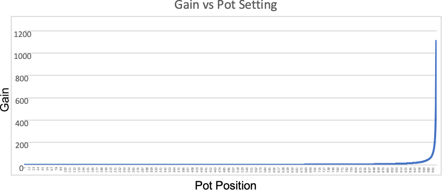
There is one problem with the voltage divider (PPISO4) version versus the two-resistor/variable resistor version (PPPAC4): linearity. The voltage divider in the PPAC4 circuit (with one side fixed and the other variable) produces a linear change in gain as you move the pot wiper from one end to the other. In the PPISO4 design, moving the pot wiper changes both the input and feedback resistor simultaneously. This produces a very non-linear plot of gain versus pot position, especially as the pot wiper moves to the point the input resistor is zero:
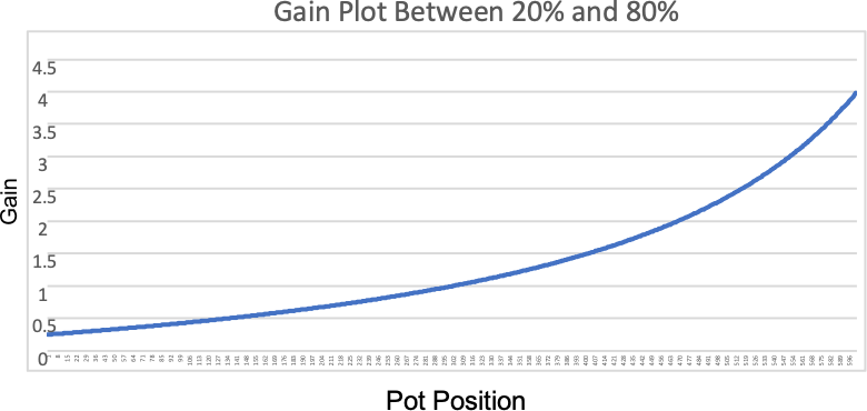
As it turns out, this circuit produces reasonable results between the 20% and 80% positions:
The optional 5kΩ resistors help solve this problem by flattening the curve a bit. They also make the SPAN pot adjustment a little more precise (similar to increasing the size of the resistor on the ZERO pot). HOWEVER, there is a big issue with adding these two resistors: you've now got three different resistors (each with their own TCR) in the circuit. This will (slightly) increase the gain drift. Furthermore, adding additional solder connections affects the overall TCR of the PCB and circuit. So adding the two 5kΩ resistors will flatten the gain curve and make it easier to adjust the gain during calibration, but at the expense of some additional drift. Another issue with adding these resistors is that they limit the maximum gain of the circuit (fixable by using smaller resistors, but that unflattens the curve a bit and makes adjustment a little more difficult). Bottom line is that you should only add these resistors if they are absolutely necessary; they may create more problems than they are worth.
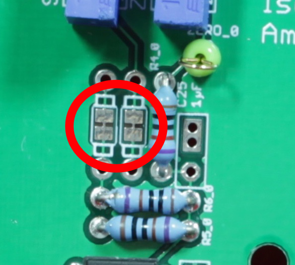
If you decide to add the resistors, note that the default assumption on the PPISO4 PCB is that they will not be installed. Underneath the resistor positions are some solder pads with traces you must cut before installing these resistors:
5kΩ is a good value if you're using 20kΩ SPAN pots. If you're using 10kΩ SPAN pots, 2kΩ would probably be a better choice for these resistors.
If you don't install these optional resistors, you should manually measure the SPAN pots before attempting to calibrate the PPISO4 board. Adjust them to the half-way point (e.g., 10kΩ for a 20kΩ pot, or 5kΩ for a 10kΩ pot). This will ensure that you're not operating at the "crazy" end of the gain curve (from which it's very difficult to begin the calibration process).