
Note: All photographs appearing on this page are freely usable for any purpose. Links to high-resolution versions of the pictures appear below each picture.
Digital Data Acquisition & Control System
PPIT
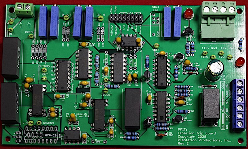
Analog (double) Isolation and Trip Board
High-resolution image
The PPIT board is a single channel analog isolation amplifier and trip board with the following features:
- Input can be single-ended voltage (±10V), 4-20mA, or differential voltage input (INA137 compatible input supporting up to ±10V differential inputs).
- Input voltage isolation (isolation of single-ended input, or voltage output from RCV420/4-20ma IC or voltage output from INA137 differential voltage input IC).
- After isolation stage, the PPIT board provides an amplification stage with high-precision/low drift OPA4227 operational amplifiers. Opamp stage provides gain and offset (span/zero) controls using low-drift potentiometers. Optional resistors allow the control of the gain/offset ranges to support a wide range or a more precise control (with a more limited range).
- Outputs from the opamp stage are available on the output header.
- An independent isolation amplifier provides an isolated output stage with its own gain/offset (span/zero) controls.
- Isolated output signal can be single-ended or differential (via DRV134 IC or a dual opamp circuit).
- Trip circuitry provides two analog comparator circuits to support a range of valid inputs. A trip can be set when the input voltage (or current) is below a certain level, above a certain level, within some range, or outside some range.
- PPIT implements the trip circuitry using a FORM-C relay. The system is configurable to use a JZC-11F SPDT relay (one set of NO/COM/NC contacts 5A @ 30vdc or 240vac) or an HK19F DPDT relay (two sets of NO/COM/NC contacts, 2A @30V or 1A @125V).
- Outputs:
- +Differential voltage out, -Differential voltage out
- +Isolated voltage out, -Isolated voltage out (can be single-ended or differential)
- +Vout, Gnd (single-ended voltage out)
- Trip (logic level), Gnd
- VLow, Gnd (voltage at which the low-range trip occurs)
- VHi, Gnd (voltage at which the high-range trip occurs)
- VTest, Gnd (voltage to be summed with the input voltage for remote trip testing)
- PreVoltOut, Gnd (Input voltage before summing in VTest)
- Inputs:
- +In (+Vin for single-ended or differential inputs, +Iin for 4-20mA input)
- -In (Gnd for single-ended input, -Vin for differential inputs, -Iin for 4-20mA input)
- +12V (power supply; can also be +15V)
- -12V (power supply; can also be -15V)
- +5V (power supply)
- Gnd (power supply)
- Open Source/Open Hardware design (Creative Commons 4.0 license).
- Stable, low-drift design.
- LED indicates when power is applied.
- Optional DIN rail brackets allow installation on 35mm DIN rails.
- DIN rail brackets are available in .STL format for 3D-printing.
Original Use Case
Originally, the PPIT was designed as a component in a nuclear fuel temperature monitoring (FTM) system. Instrumented fuel rods (IFEs, containing a K thermocouple bonded to the fuel rod) were wired to a thermocouple amplifier that produced a voltage signal representing -200C to 1350C (the range of a K Thermocouple). That voltage arrived at the PPIT +In and -In inputs as a ±5V differential value. The INA137 IC converted this differential signal to 0 to 5V (the INA137 IC has a gain of -6dB, or 0.5) and then ran the value through an isolation amplifier to isolate the thermocouple circuit from the FTM. After isolation, the gain and offset circuitry on the PPIT board scaled the voltage to 0-5V, representing 0 to 1000C (technically, it scales the input to some negative voltage up to some voltage higher than 5V, but 0 to 5V is the range used by the FTM, and reactor fuel temperatures are never below 0C or above 1000C; the tank would be frozen at 0C and the fuel elements melt at around 950C).
The 0 to 5V output is sent to an analog-to-digital converter in order to display the fuel rod temperature on the FTM's display screen. This voltage is also sent to the comparator circuitry to generate a trip (that will SCRAM the reactor) if it exceeds some set point (set by a potentiometer in the comparator circuit). Note that the trip circuitry is pure analog. Software does not (with one exception) control the trip circuitry; software does not make the descision to SCRAM the reactor, that decision is made by hardware (to reduce qualification issues when attaching the FTM to a reactor).
There is an auxiliary voltage input on the PPIT board that the circuitry sums with the voltage arriving from the IFE thermocouple. This allows an external test circuit (typically driven by a computer programming this voltage with a DAC) to test the PPIT's ability to generate a trip in response to a high temperature. The computer (or external test circuit) ramps up this test voltage, measures the sum of the two voltages, and then determines whether a trip has occurred (by looking at the trip logic output pin on the PPIT). Arguably, this means that software can control the SCRAM circuitry. However, the computer (or external test circuit) cannot prevent a SCRAM from occuring, it can only cause a premature SCRAM (by sending in a higher temperature voltage than exists at the IFE). Therefore, it is never the case that the fuel rods would exceed their temperature limits without the FTM generating a trip (one could be generated when the temperature is below the hardware set point, but that's not a safety-critical failure).
In addition to providing a voltage for use by the FTM's CPU, the PPIT also provides an isolated output amplifier circuit to allow the transmission of the temperature (via an output voltage) to some external circuitry that is monitoring the fuel temperature (such as an ADC input on a TRIGA reactor digital console). The output is isolated to prevent any interference between the external system and the FTM.
Additional Use Cases
The PPIT is useful any time you need a hardware (analog) trip circuit and isolation amplifier monitoring a safety critical system. It is particularly useful in safety-critical systems where software is difficult to prove correct or a regulating agency (such as the NRC) requires expensive validation and verification of a software system before allowing its use.
Of course, the PPIT is usable anywhere an analog trip circuit is required, though the dual isolation amplifier design may be overkill for many projects.
Instrumentation Quality
The PPIT has been designed to produce stable readings and trip settings over a wide temperature range and over time. By using appropriate components (instrumentation-quality opamps, resistors, and pots), highly repeatable results are possible.
Of course, if such quality is unnecessary, you can use low-cost ("jellybean") opamps and resistors and dramatically reduce the cost of the parts needed for construction.
Build Options
The PPIT can be configured during assembly to handle many different scenarios. For example, you can select single-ended, differential, or 4-20 mA current-loop inputs by choosing which components you install on the board. If you don't need the isolated output amplifier, you can leave off the compnents for that circuit without affecting the performance of the rest of the system. Likewise, if you don't need an isolated input, it's very easy (just a few jumper wires) to bypass that portion of the design.
The gain (span) and offset (zero) potentiometers on the PPIT can operate in one of two modes: widest possible values (gain or offset), or greater precision. By default, the circuit design assumes the user will want to choose the greatest amount of gain and offset voltages. By cutting some jumpers and adding some 4.7KΩ resistors, you can modify the circuit to produce a more limited range of gain or offset, but allow a more precise setting of these values using the multi-turn potentiometers.
The circuit design provides for two different differential voltage output options (in addition to singled-ended outputs): you can use a DRV134 differential output driver (very high quality) which produces a +6dB gain (a gain of two) output for reducing noise (the preferable option). However, the DRV134 produces both negative and positive voltages on its output pins. Certain ADCs (e.g., ADS1115) do not like negative voltages on their output pins, so a second circuit option uses a pair of opamps to generate the differential circuit. It's not as precise, and requires an expensive potentiometer, but it will generate a differential output where both output voltages are always positive with respect to ground.
The build instructions will describe how to select this options during assembly.
Bill of Materials (BOM) for the PPIT board
I/O-independent materials:
- Optional (16) Test pins
- (7) 0.1 µF bypass capacitors
- (10) 1 µF tantalum capacitors
- (2) 470Ω 1% metal-film resistors
- (7) 10KΩ 1% metal-film resistors
- (2) 100KΩ 1% metal-film resistors
- (2) 200KΩ 1% metal-film resistors (can substitute 100KΩ for greater hysteresis in comparator circuit)
- (3) 20KΩ 0.1% 15 PPM/C resistors (high precision, e.g., TE Connectivity YR1B20KCC)
- (1) Vishay TDP16032002AUF resistor array (8x20KΩ resistors in a DIP package) -or- (8) 20KΩ 0.1% 15 PPM/C resistors (high precision)
- (2) 1N4148 diodes
- (2) 2N2222 NPN bipolar transistors
- (2) BF256B JFET transistors
- (2) Red 5mm LEDs
- (2) OPA4277 opamps
- (4) 20KΩ multi-turn trim pot (Bourns 3005P-1-203 20KΩ 50 PPM/C or, better yet, Vishay 71-1280G-20K-K 15 PPM/C)
- (2) ISO122 isolation amplifier ICs
- (1) JCZ-11F / 005-1Z 5V SPDT relay -or- (1) HK19F-DC 5V-SHG DPDT 5V relay
- (1) 1000 µF 35V low ESR electrolytic capacitor
- (3) Meanwell DPB09A-15 isolation power supplies
- Optional: (8) Vishay CMF554K7000BER6 4.7KΩ 0.1% 25 PPM/C 1/2W resistors
- (1) PPIT PCB
- (1) 16-pin (2x8) male header
- (1) 2-pin (1x2) male header
- (2) 3-pin screw terminal (5mm/0.2" centers)
- Optional: one set of horizontal 35mm DIN rail mounts for DAQ boards
Additional Parts for Differential Input (using INA137):
- (2) 1 µF tantalum capacitors
- INA137 (differential receiver IC)
Additional Parts for 4-20mA Current Loop Input:
- (1) 3-pin header
- (1) RCV420 (4-20mA receiver IC)
Additional Parts for Single-ended Input:
- (2) short jumper wires
Additional Parts for Differential Output (using DRV134):
- (2) 1 µF tantalum capacitors
- (1) DRV134 differential transmitter IC
Additional Parts for Differential Output (using opamp):
- (3) 20KΩ 0.1% 15 PPM/C resistors (high precision)
- (1) 20KΩ multi-turn trim pot (Bourns 3005P-1-203 20KΩ 50 PPM/C or, better yet, Vishay 1280G-20K )
- Note: this circuit uses two opamps that are part of the OPA4227 IC
Building First Article:
When building your first unit, you can substitute 1% metal film resistors for the 0.1% 15 ppm (high-precision) resistors and the resistor array. You can also substitute a LM324 opamps for the OPA4277 opamps and install standard (low-cost) potentiometers to reduce the cost of the prototype. This will allow you to test the prototype PCB for considerably less money (sadly, the isolation amplifiers and isolation power supplies, which are expensive components, will still be necessary.
PCB Availablity
Note: If you only want a few PPIT PCBs, contact Plantation Productions (randy@plantation-productions.com) to see if there are any in stock. Bare boards are $25 each plus shipping; fully assembled and tested boards are $750 each. If you need more than a couple PCBs and you're not in a huge hurry, it costs about $150 plus shipping (plus about 4-6 weeks) to have a set of 10 manufactured and shipped to you from China. I use Seeed Studio Fusion PCD service (https://www.seeedstudio.com/fusion.html). The PPISO4 PCBs are four-layer boards. Here are the files:
| Description | Link |
|---|---|
| Gerber files for PCB (provide these files to Seeed Studio or your personal PCB manufacturer) | PPIT Gerber Files for PCB |
| Eagle schematic capture and PCB layout files. Use these if you want to modify or enhance the PPIT design, or re-layout the PCB using Eagle | PPIT Eagle files (Schematic and board layout) |
| On-line schematic (PDF format) | |
| PP Standard DIN rails (STL format for 3D printer) | PP Standard DIN Rail Brackets 3D printer files |
| Adjustable DIN rail bracket (STL format for 3D printer) | Adjustable DIN Rail Bracket 3D printer file |
Revision History
Rev 1:
Converted PP420IT design to PPIT.
Included the following changes from PP420IT Rev 4:
Changed relay to DPDT (+ overlaid SPDT).
Added extra pair of opamps and made Vout output.
Lengthened RC constant for relay filter and added more buffering.
Went 4-layer. Redesigned for better temperature stability.
Replaced a pair of 2n2222 BJTs with BF256B JFETs to handle higher voltage.
Added hysteresis to comparator inputs.
Rev 2:
Relaid out the SPDT relay.
Swapped NC and COM pins on DPDT relay.
Changed values on pots.
Changed LED resistors to 470Ω.
Rev 3:
Changed 220Ω resistor to 470Ω.
Changed optional (20K) resistors to 4.7K
Changed R1 from 10K to 20K (to use the same 15PPM resistors as in the opamp circuits).
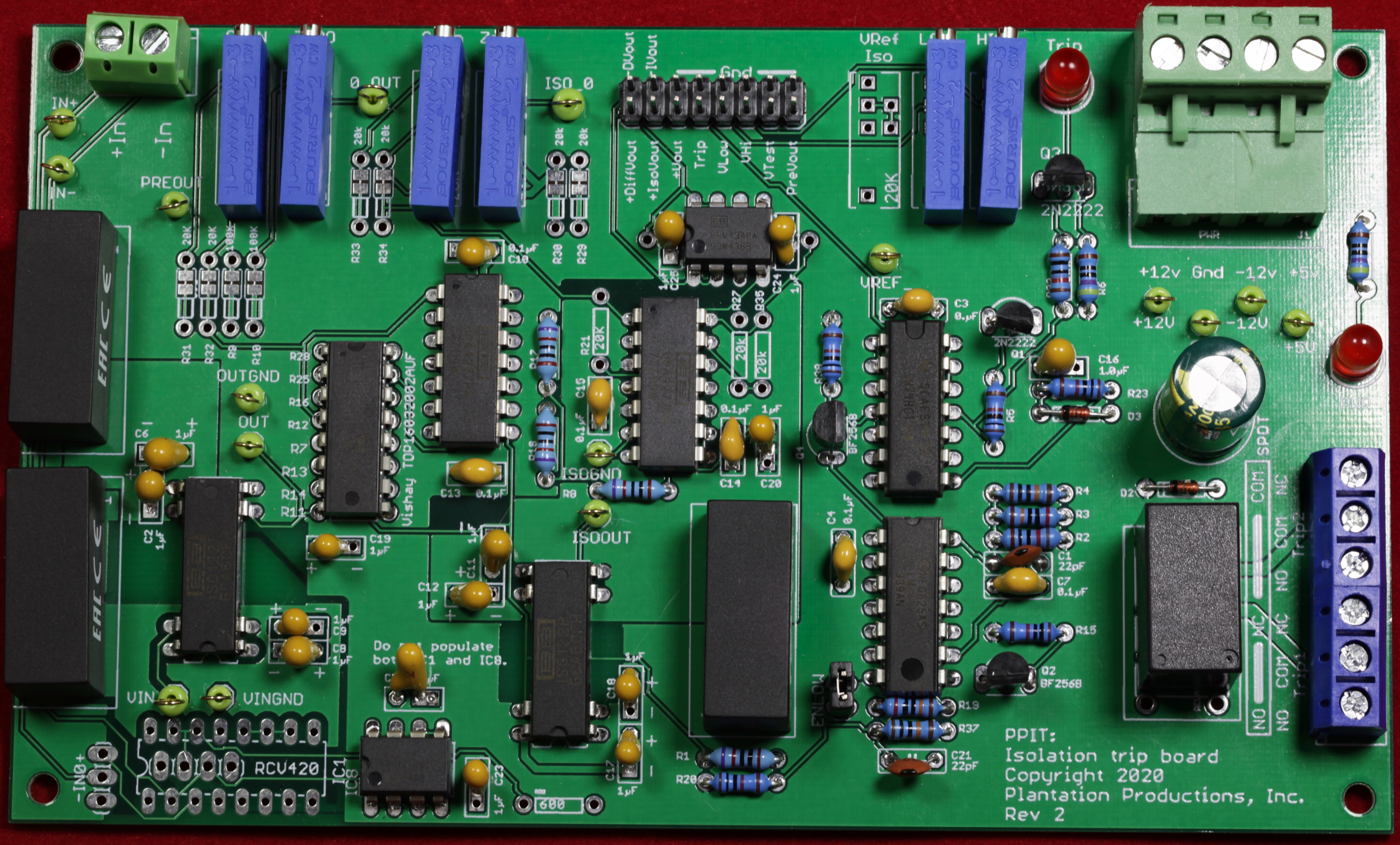
PPIT Board Layout
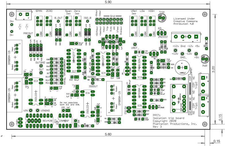
Connections
The PPIT provides a 2-pin screw terminal for input connections (+IN and -IN).
The output connector (2x8 header) has the following pinout:
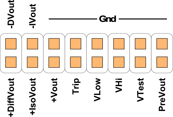
- The +DiffVout/-DVout pins provide an isolated differential output (when the differential output circuitry is added to the board).
- The +IsoVout/-IVout pins provide an isolated output. Note that only one of +DiffVout/-DVout and +IsoVout/-IVout can be effectively used on a PPIT board. Both are isolated, the +IsoVout/-IVout pins provide a single-ended output signal whereas the +DiffVout/-DVout provide a differential output.
- The +Vout/Gnd pins provide the standard, non-isolated, single-ended output from the PPIT board. This output is isolated from the input and may have an appropriate gain and offset applied to the input voltage.
- The Trip/Gnd pins provide a logic-level signal indicating that a trip has occurred. The Trip pin is logic high when no trip occurs and is logic low when a trip is active (that is, this is an active low signal). Nominally, this pin puts out around 5V for a logic high and near 0V for a logic low.
- The VLow/Gnd pins provide the low-level trip voltage for the system. When +Vout is at or below this voltage level, the system registers a trip. Note: though the VLow pin always provides the low-level trip voltage, low-level trips are only active on the PPIT board if the ENLOW header contains an installed jumper. Without this jump the system disables low-level trips.
- The VHi/Gnd pins provide the high-level trip voltage for the system. When the +Vout voltage is above this level, the system will register the trip. Unlike low-level trips, high-level trips are always active (though they can be effectively disabled by setting the VHi value to a very high voltage).
- The VTest/Gnd pins are an input to the system. The system sums the VTest and input pin values to produce the value appearing on the +Vout pin. This allows external circuit to test the proper operation of the trips by putting a sufficiently high voltage on this pin to trip the high-level trip.
- The PreVout pin provides the +Vout signal without the summation of the VTest voltage.
Test Pins
The PPIT has 13 test pins:
- VIN/VINGnd: The input voltage appears on these test pins (after processing by the 4-20mA or differential input circuits). Typically, this will be between -10V and +10V.
- Out/OutGnd: these are the output voltages from the first stage (input) isolation amplifier. Note that OutGnd is the same as the system ground.
- PreOut: this is the output from the PPIT before the VTest voltage added in; note that this is the same signal appearing on the PreVout pin and is measure relative to the system ground.
- 0_Out: this is the output voltage from the ZERO pot for the main opamp circuit. The voltage is measured relative to the system ground.
- ISO_0: this is the output voltage from the ZERO pot for the isolation output circuitry. The voltage is measured to ISOGND (the ISOGND test pin).
- ISOOUT/ISOGND: this is the output from the output isolation amplifier. IsoOut is measured relative to IsoGnd.
- VRef: the output from the VRef pot (used only in certain configurations of the PPIT).
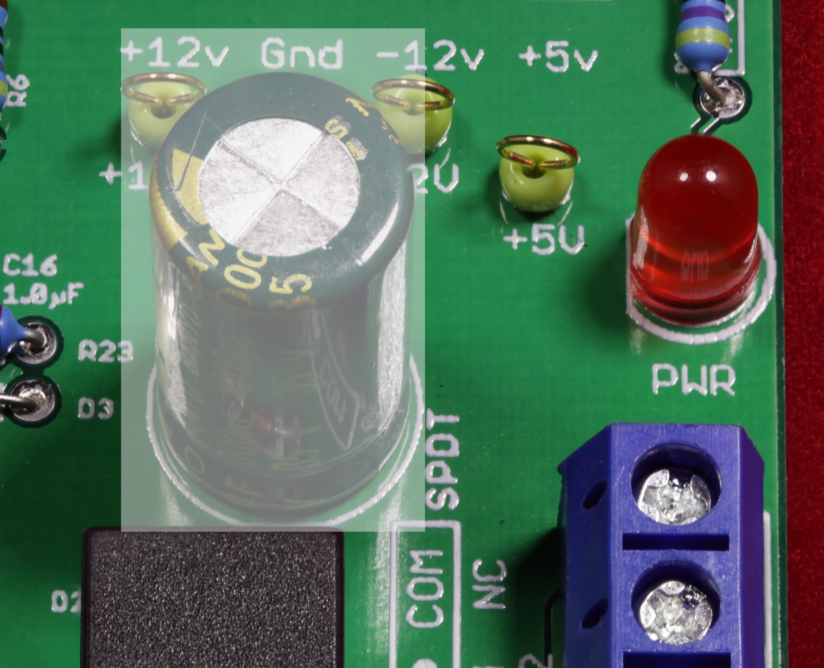
- +12V, Gnd, -12V, +5V: System power supply voltages.
In addition to the 16 test pins (four per channel), there are three additional pins connected to the power supply signals (Gnd, +12V, and -12V).
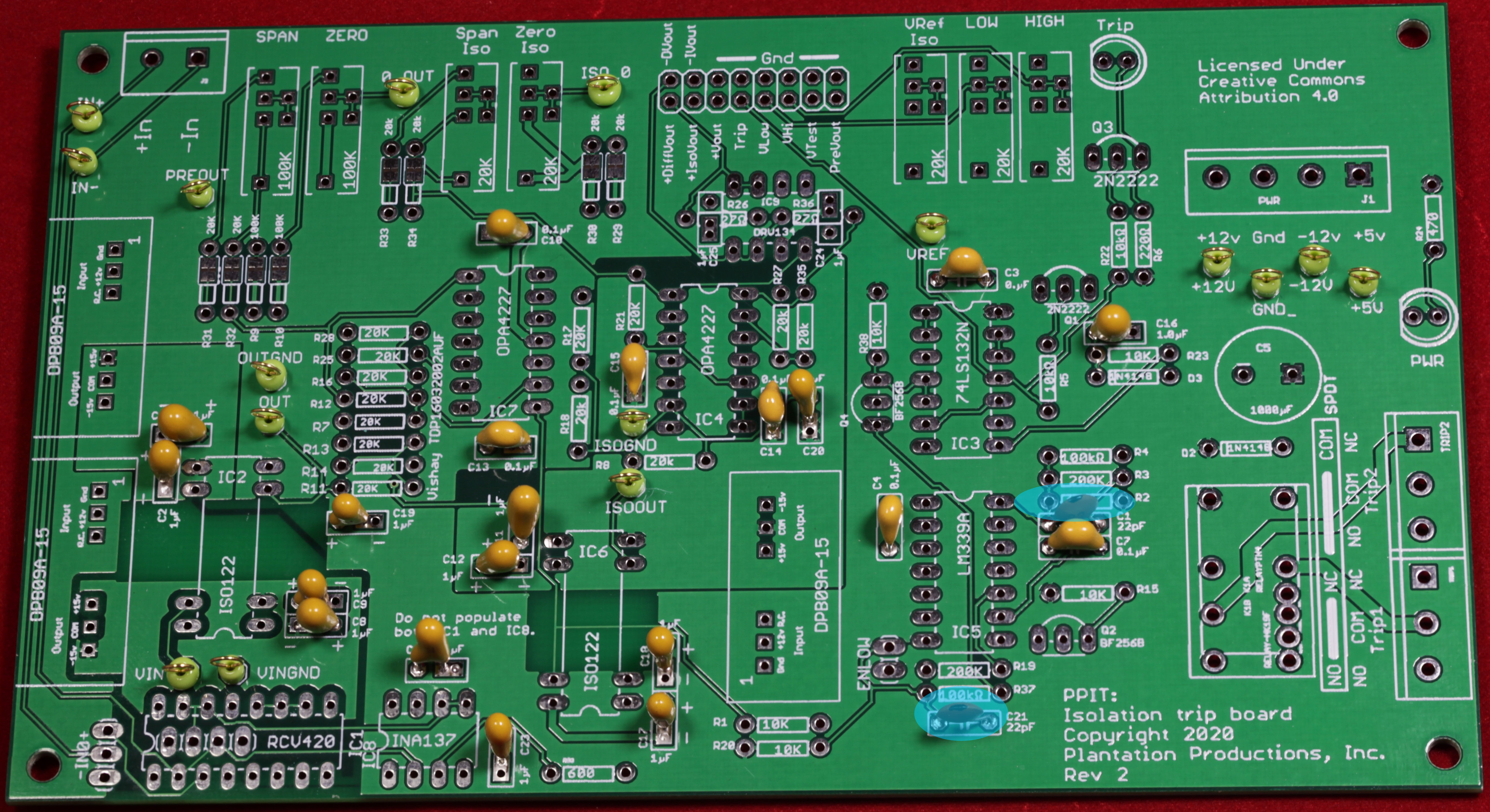
Building a PPIT Board
Note: the following images describe the construction of a PPIT Rev 2 board. The current revision (Rev 3) contains relatively minor (mainly silkscreen) changes so these instructions apply as well. Where there are differences, these instructions point out the differences (along with other assembly options).
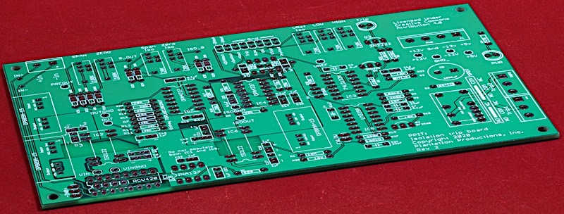
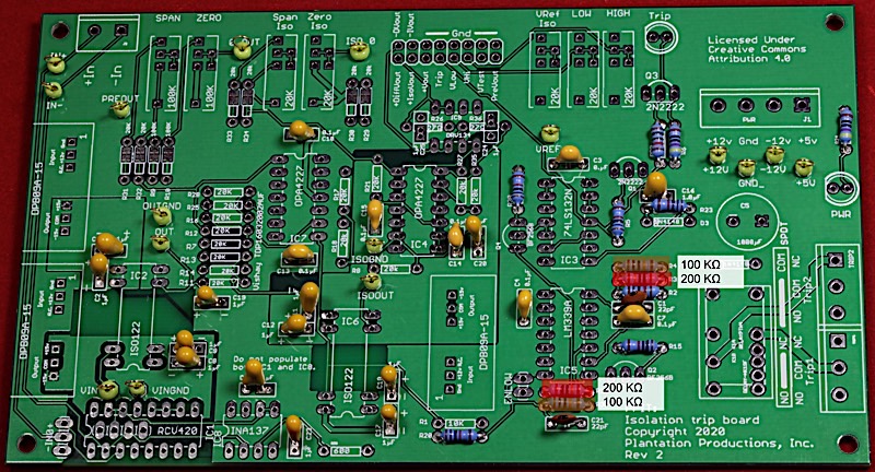
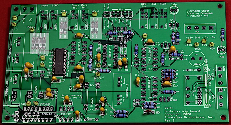
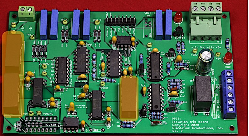
Here's the bare PPIT PCB (printed circuit board):
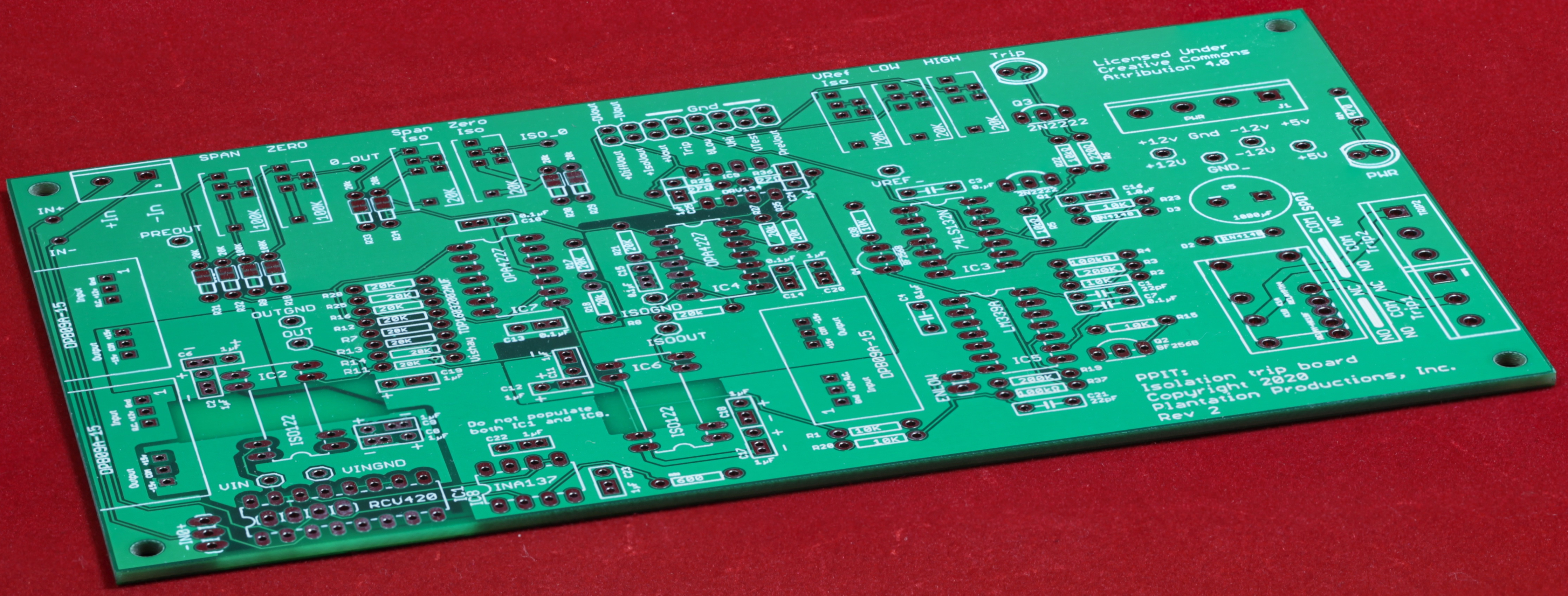
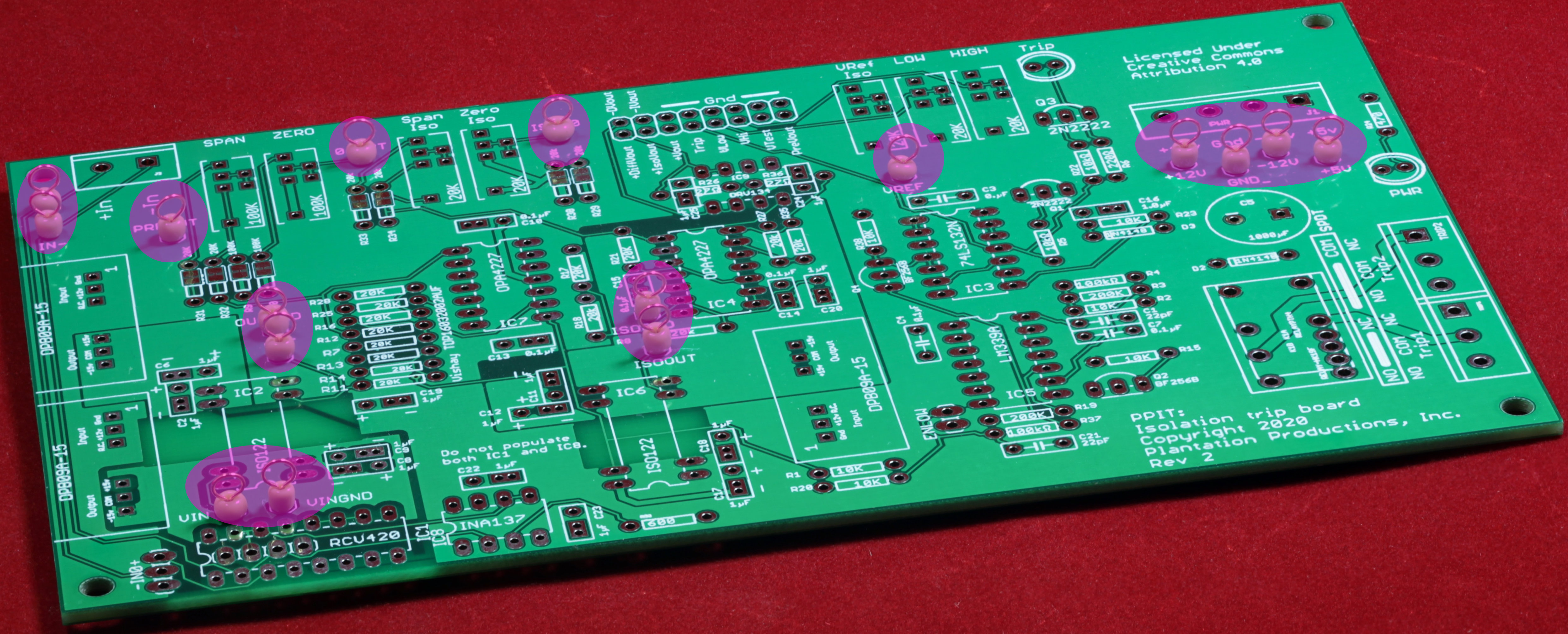
- The usual build process is to build a board from "the bottom up." This means to first install those items closest to the PCB and work you way up to larger objects on the PCB. The smallest items on the PPIT board are the 16 test pins, so solder them onto the board first (test pins are optional, skip this step if you are not putting them on the board):
High resolution image
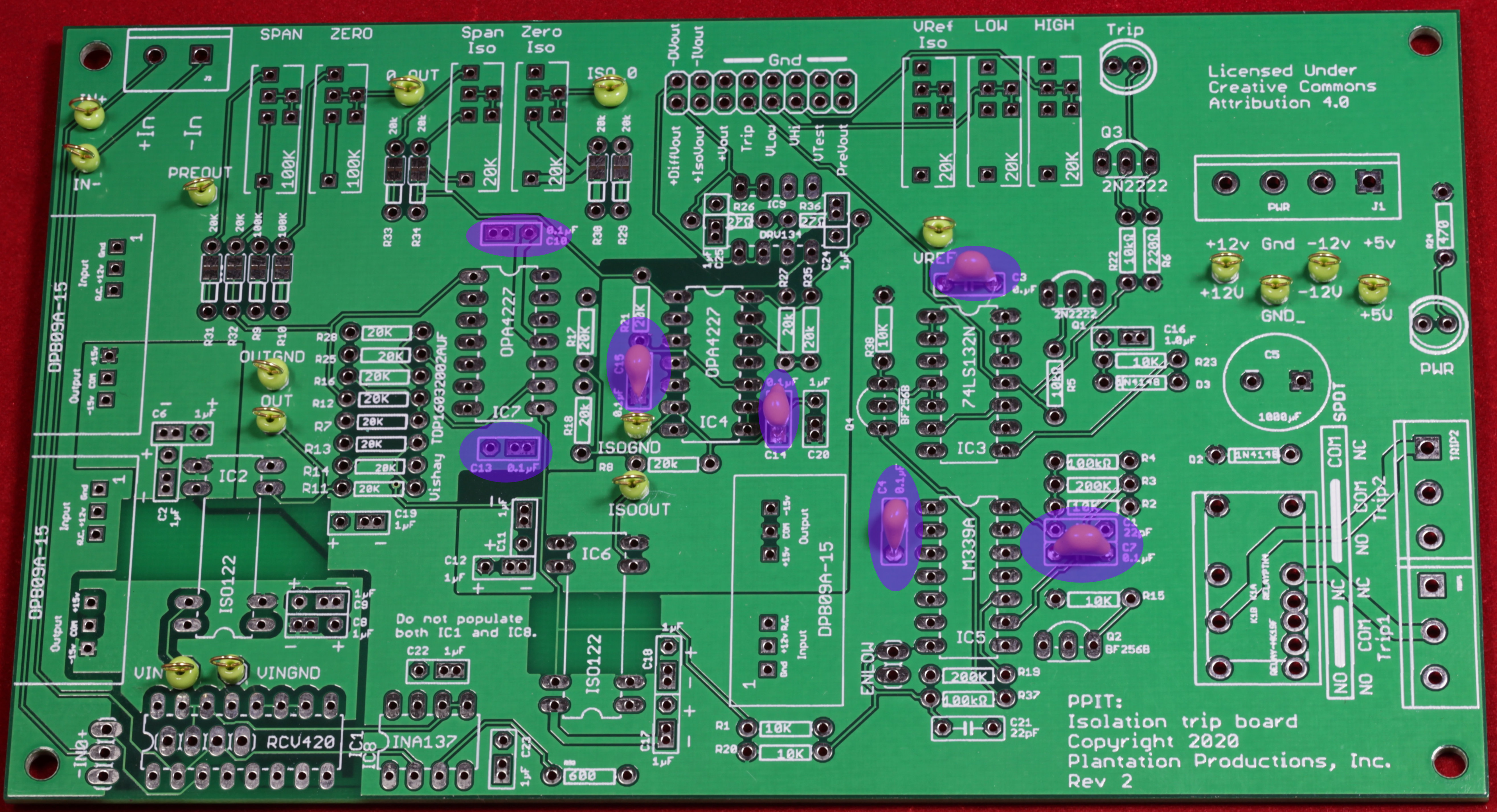
- Next, solder on the seven 0.1µF bypass capacitors.
Note: if you do not need isolated or differential outputs (+DiffVout/-DVout and +IsoVout/-IVout), you do not need to install the C14 or C15 capacitors.
High resolution image
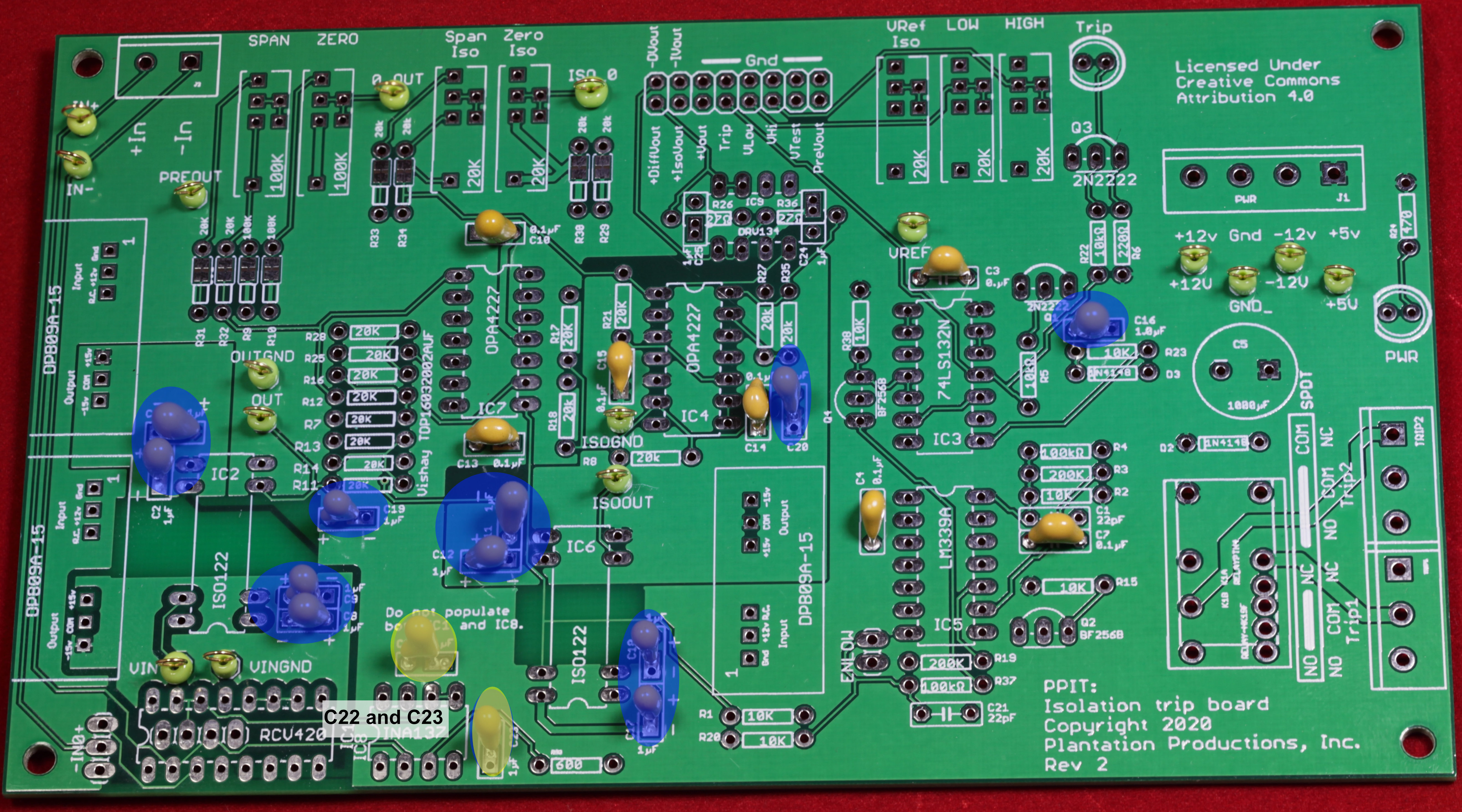
- Next, install the 11 or 13 1µF Tantalum capacitors. Note that tantalum capacitors are polarized. The short pin (-) must go in the pad with two holes on it (usually marked with a "-", but not always). If you are building a board with differential inputs, you will need to install two additional 1µF Tantalum (for a total of 13) in the C22 and C23 positions.
Note: if you do not need isolated or differential outputs (+DiffVout/-DVout and +IsoVout/-IVout), you do not need to install the C20 capacitor.
High resolution image
- The next step is to install the 22 pF filter capacitors on the comparator circuit.
High resolution image
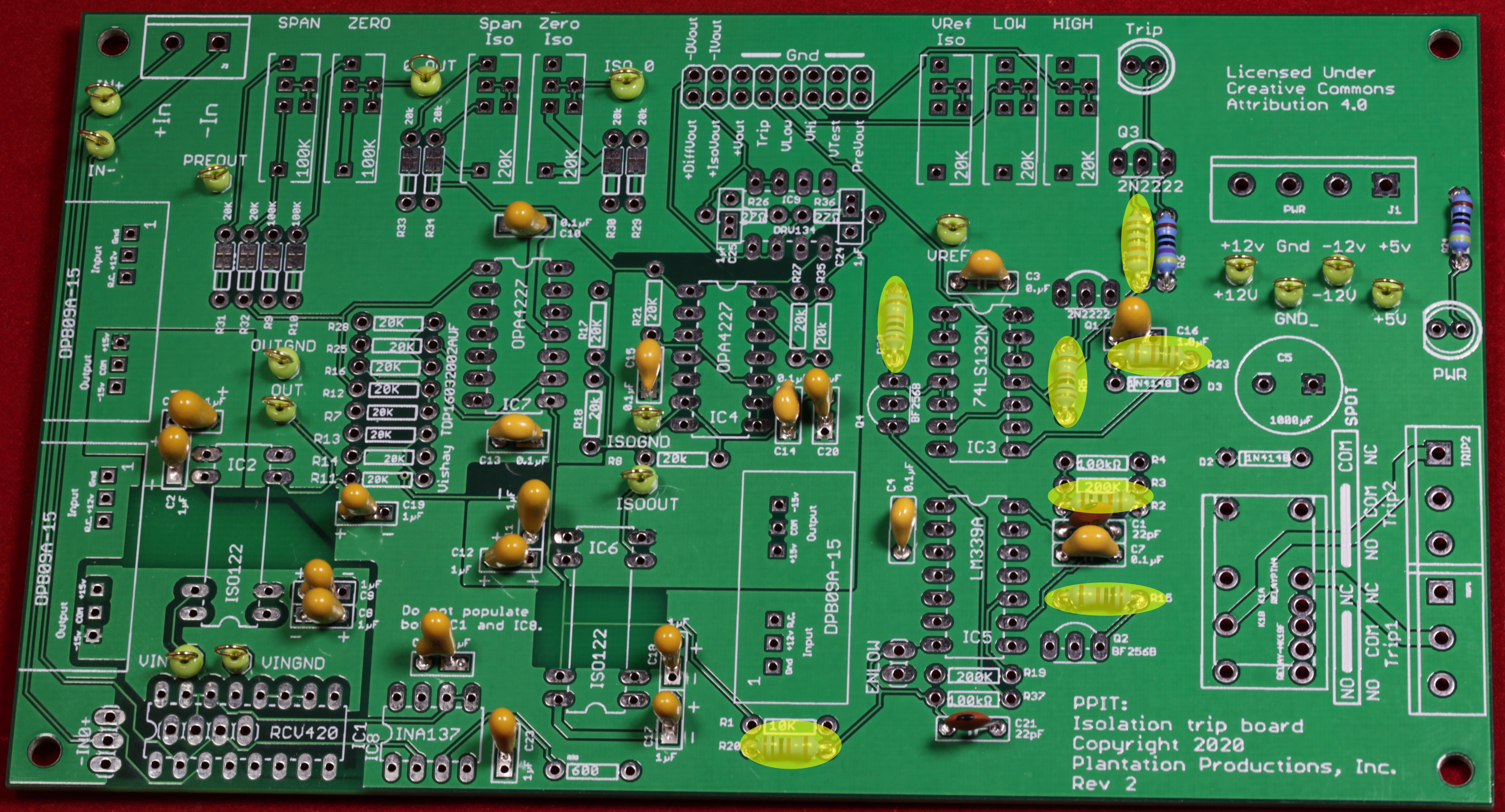
- The next thing to install are the resistors. The first two resistors to install are the 470Ω (R6 and R24). These control the current flowing into LEDs; they are listed as 1% metal-film resistors in the BOM, but they are not that critical; any jellybean 470Ω (or thereabouts) resistor will work fine here. Note that on the Rev 2 board, R6 was listed as 220Ω. This was changed to 470Ω in Rev 3 (LED will be a little dimmer, but last longer).
High resolution image
- Next, install the seven 10KΩ 1% metal-film resistors. Note that R1 is labelled 10K on the Rev 2 board; this has been changed to 20K on the Rev 3 board. While a 10K resistor would work fine here, it has to be a 0.1% 15PPM/C resistor. R1 was changed to 20K (which also works fine) to match the specification of the other 20K resistors on the PCB.
High resolution image
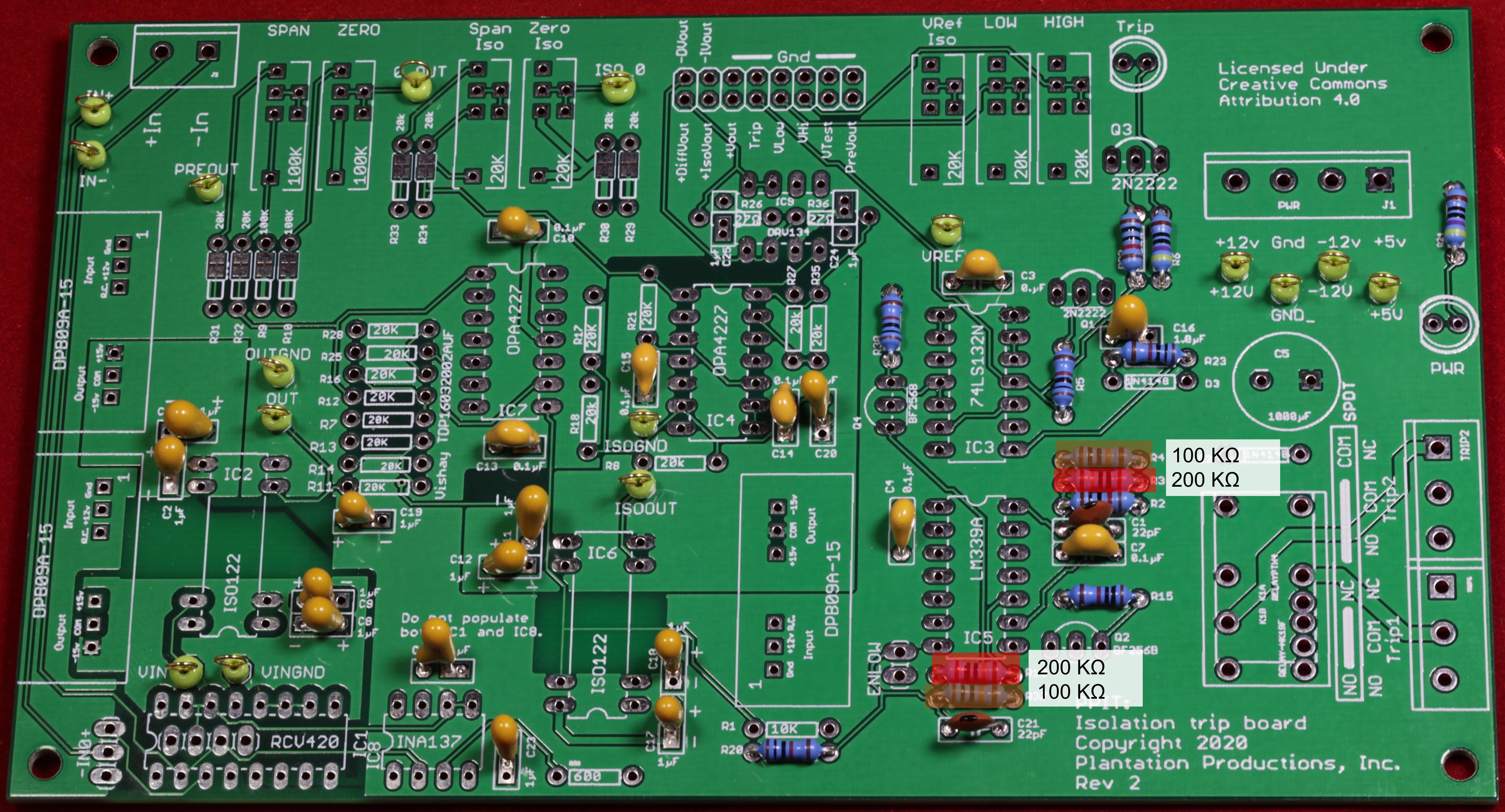
- Next, install the two 100KΩ and two 200KΩ 1% metal-film resistors. Note that the 200KΩ resistors provide feedback for hysteresis to the comparator circuit. This hysteresis prevents the relay from "chattering" whenever the input voltage is around the trip settings. You can increase the hystersis, if necessary, by using a lower ohmage resistor in place of the 200KΩ resistors (e.g., using 100KΩ for all four of them).
High resolution image
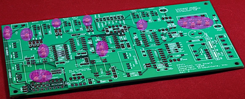
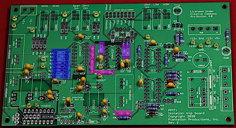
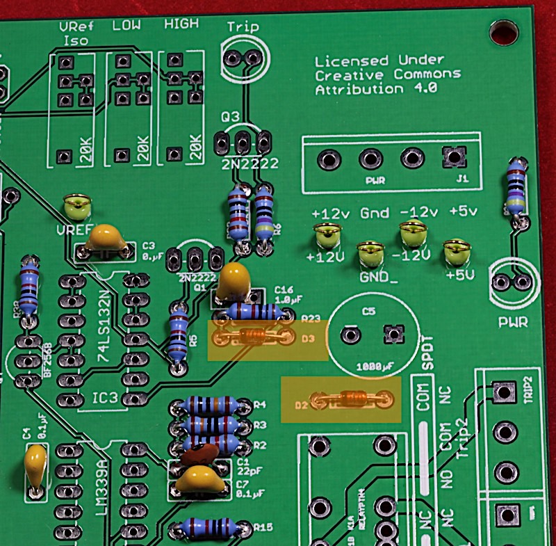
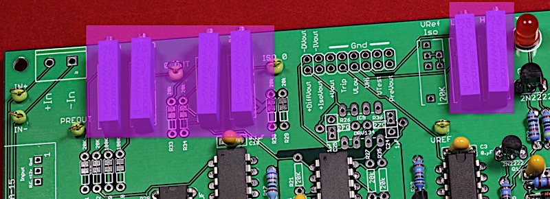
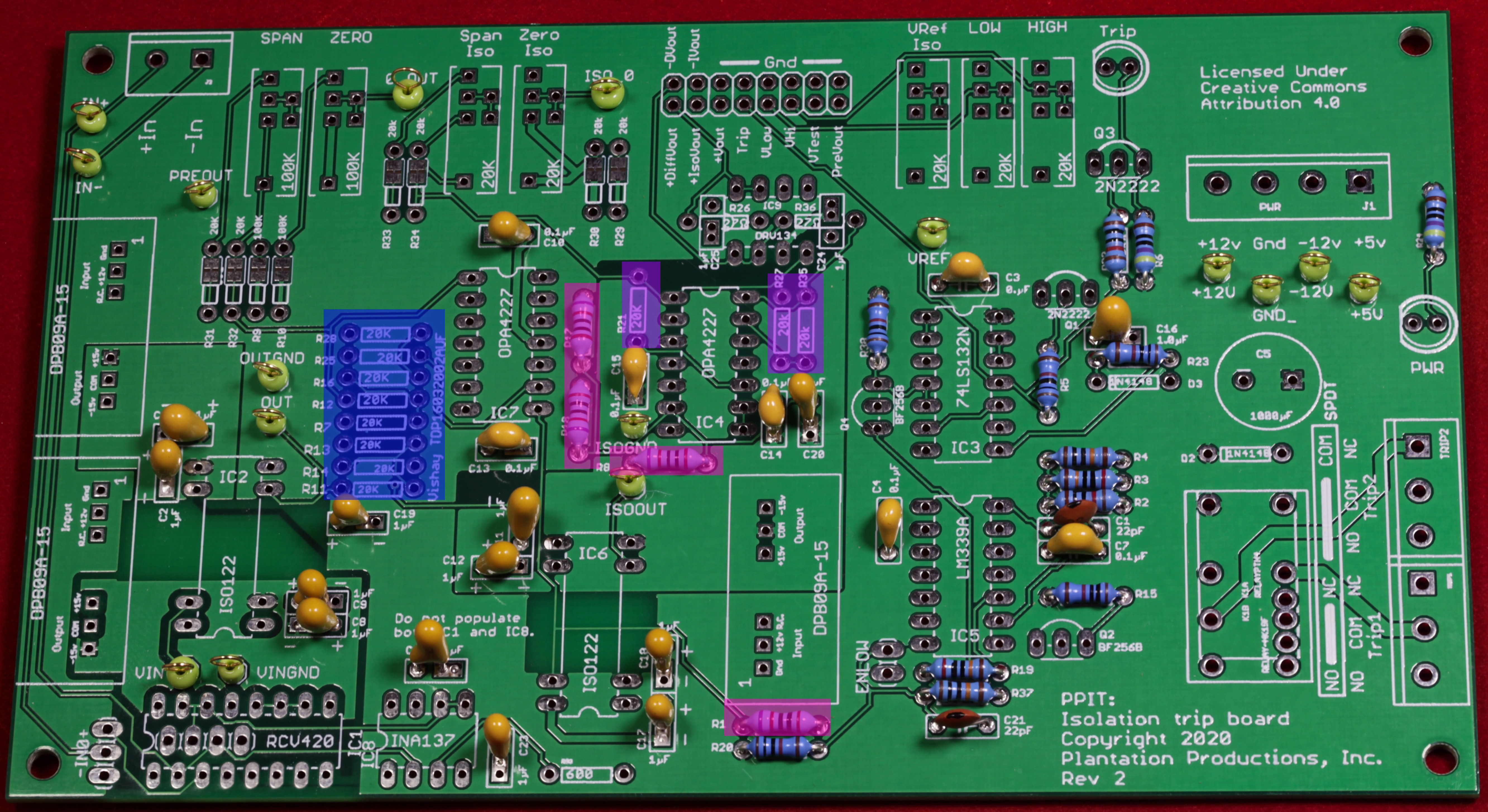
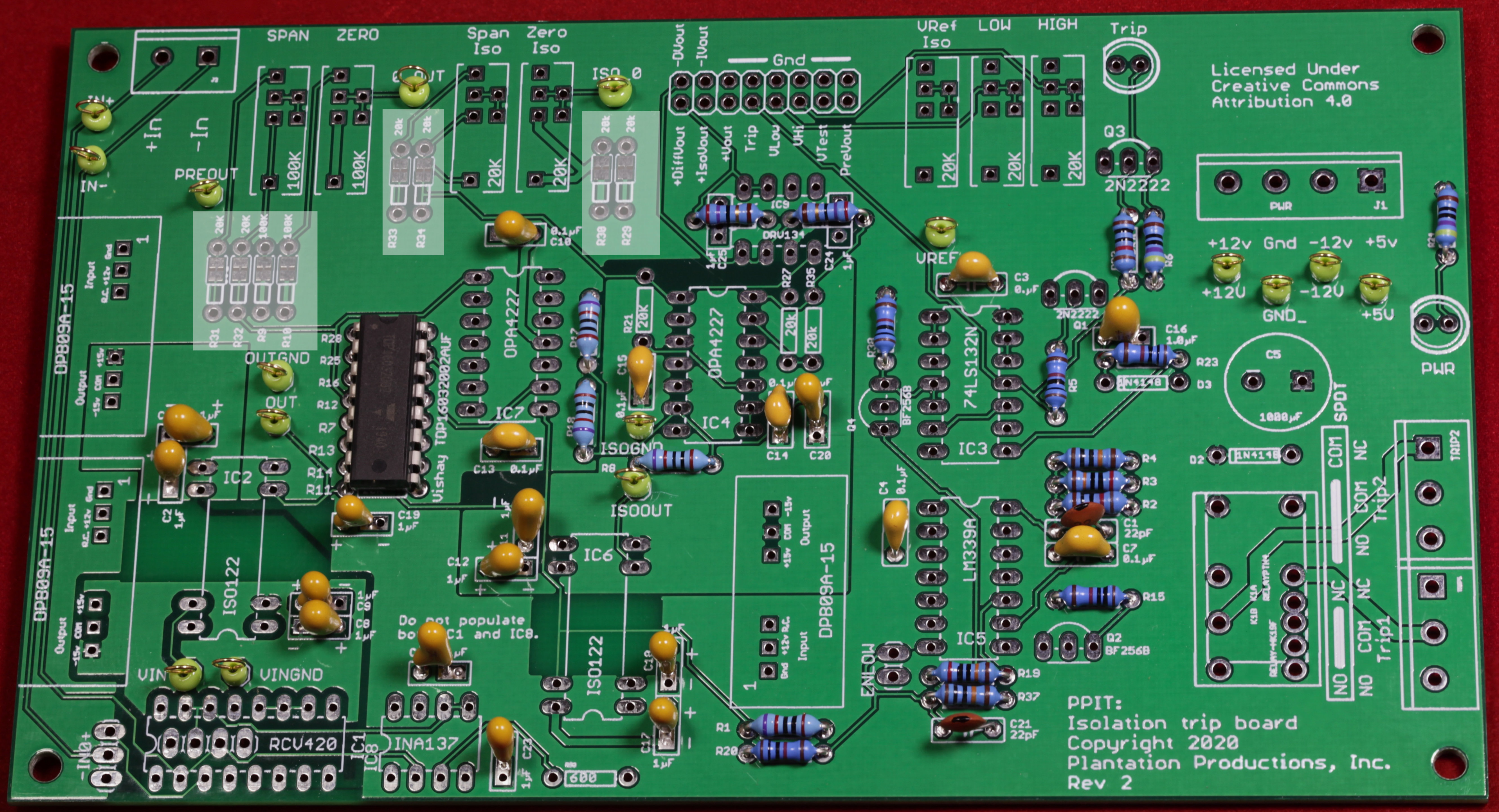
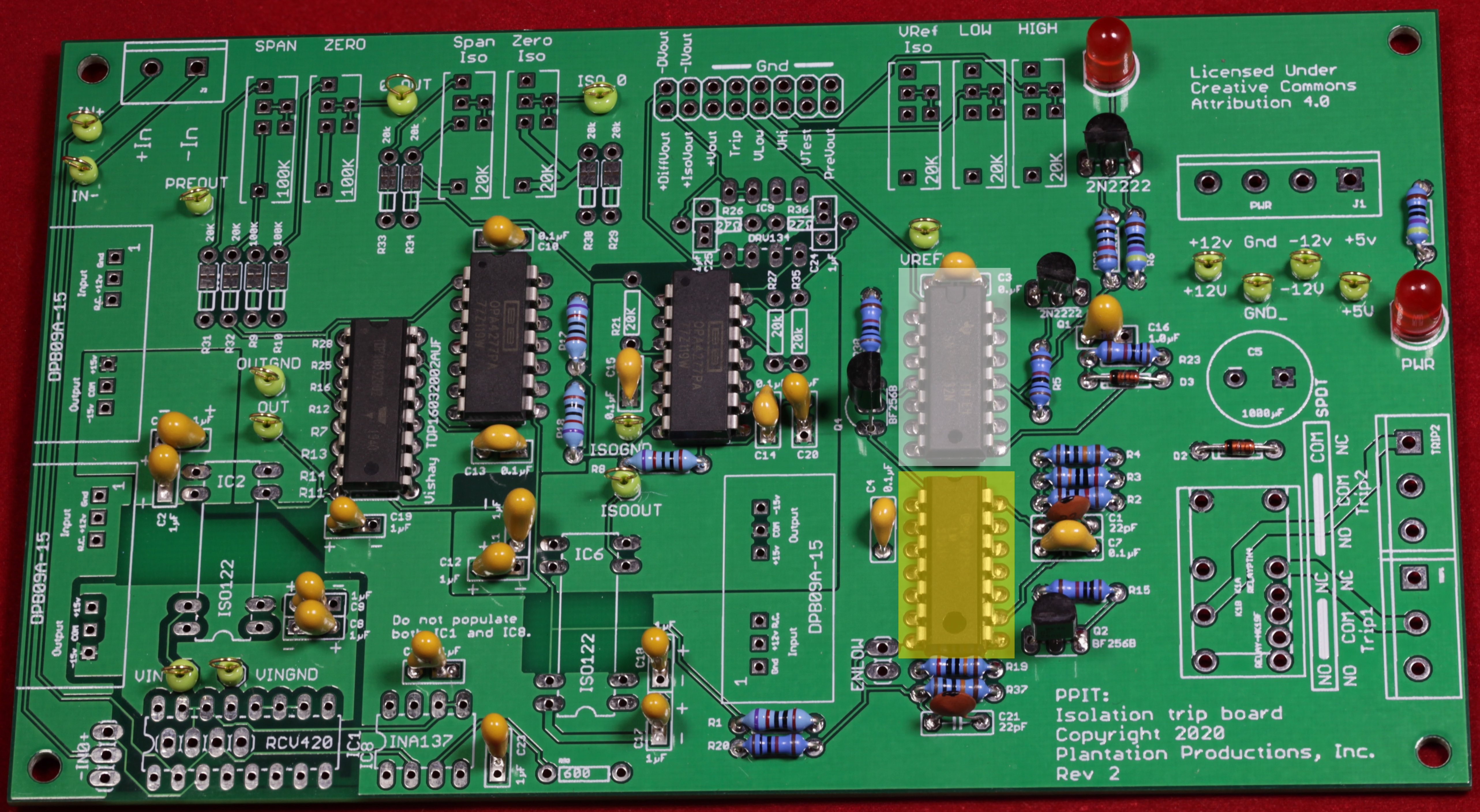
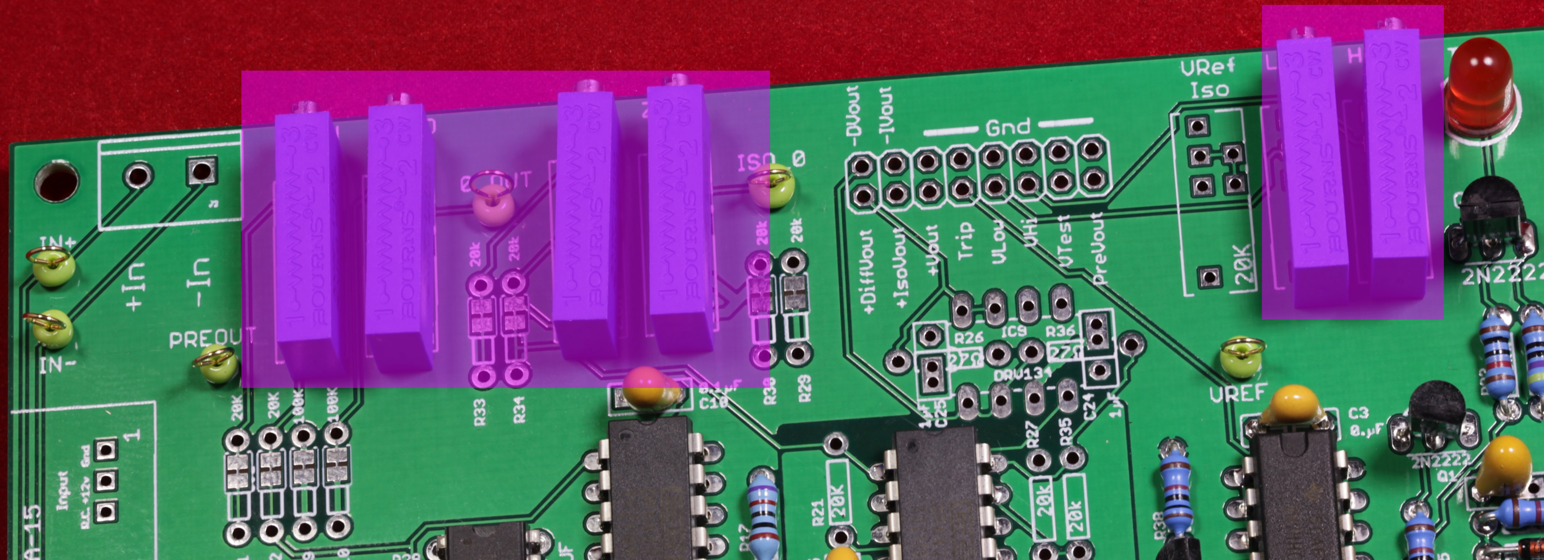
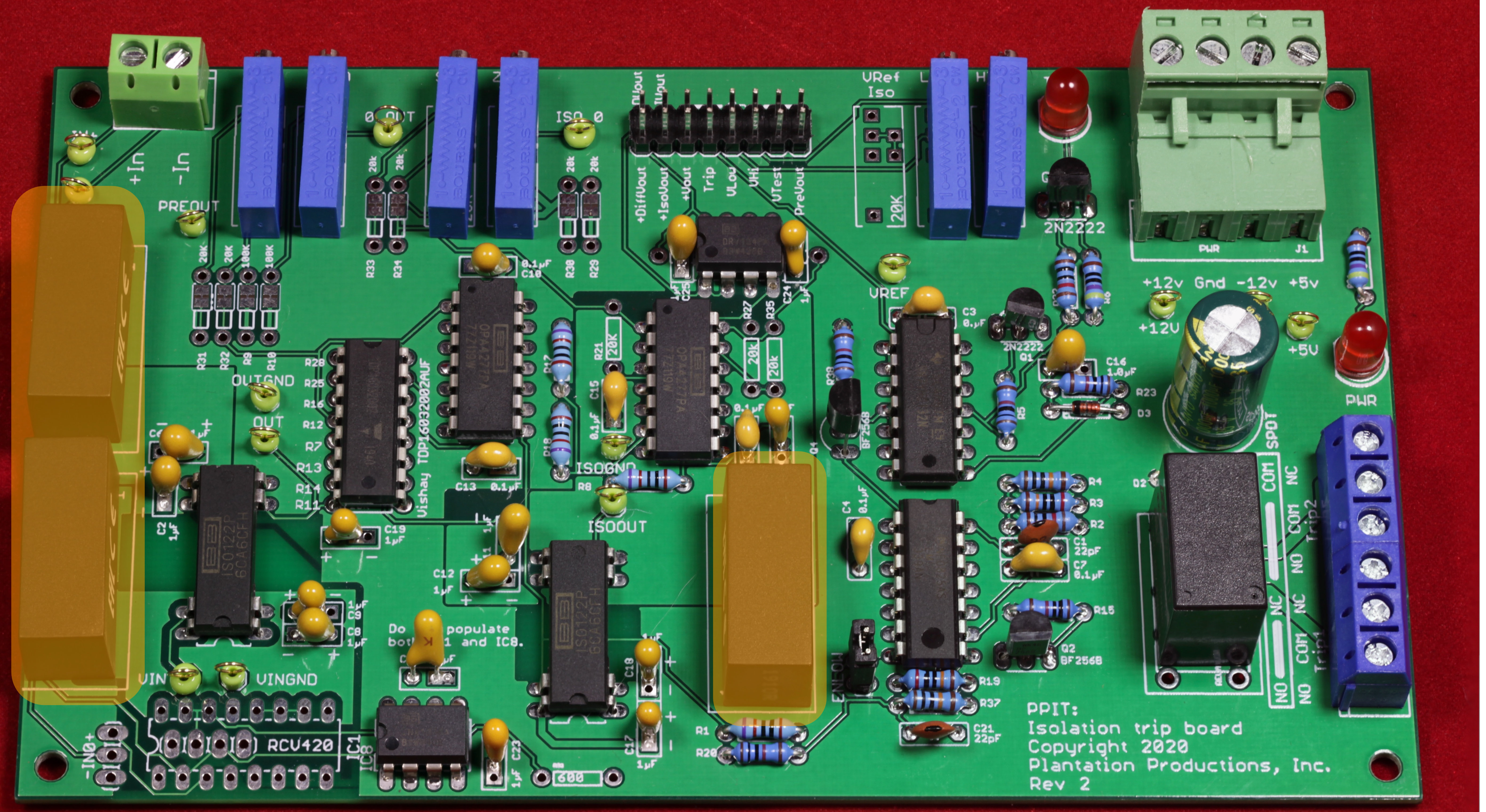
- Next, install the 20KΩ 0.1% 15 PPM/C resistors. These are very precise, instrument-quality resistors (and tend to be expensive, costing anywhere from $0.30 to a couple dollars each, depending on the brand and who you buy them from). You'll need to install anywhere between four and 15 of these resistors, depending on how you're setting up the board. Resistors R1, R8, R17, and R18 always get these resistors installed. Install three of them in R32, R27, and R35 only if you are building a unit that produces a differential output using the opamp circuit (generally for use as inputs to ADCs that cannot accept negative voltages). The picture below does not show these resistors installed (because it's not being built for that output type). Finally, there are eight 20KΩ resistors, R7, R11, R12, R13, R14, R16, R25, and R28 that could also take these resistors. However, those eight resistors are arranged on the PCB to allow the installation of a Vishay TDP16032002-1940 resistor array (which contains eight 20KΩ resistors in a DIP package). The advantage of the Vishay resistor array is that all the resistors are in the same package and their temperature tends to change in sync with one another (producing a better PPM/C rating in real life). While the Vishay package is typically more expensive than the discrete resistor (especially if you can get them for less than $1.00 each), you will typically get more stable outputs from the PPIT by using the resistor array. The magenta colored resistors below are the four that must be installed, the purple rectangles cover the locations that must be installed when using the non-negative-going differential output circuit, and the blue box covers the eight locations where the Vishay array or eight 20KΩ resistors would go.
Note: if you do not need isolated or differential outputs (+DiffVout/-DVout and +IsoVout/-IVout), you do not need to install the R8, R17, and R18 20KΩ resistors.
High resolution image
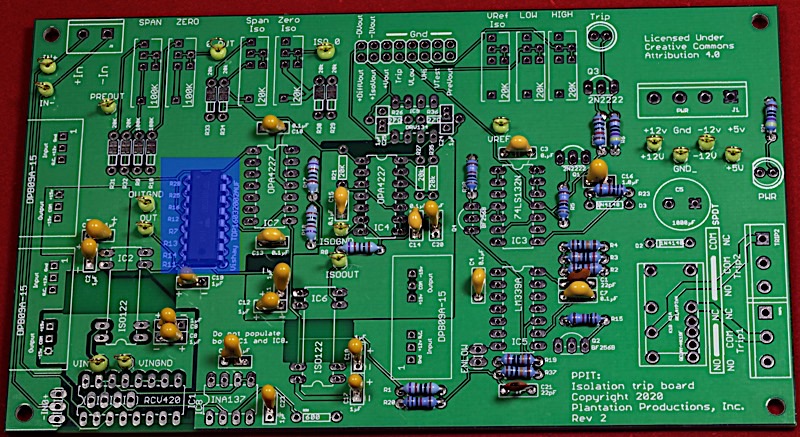
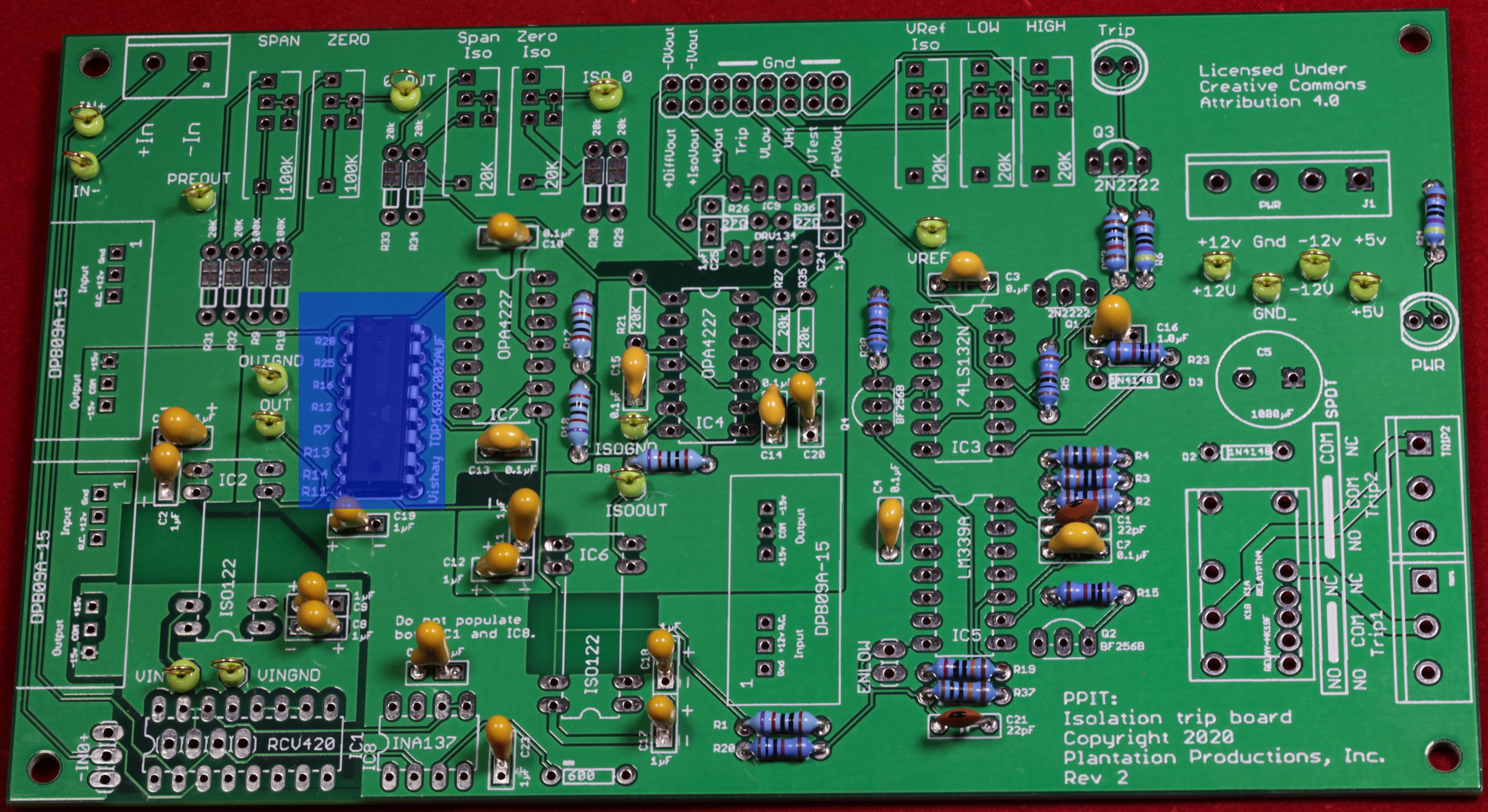
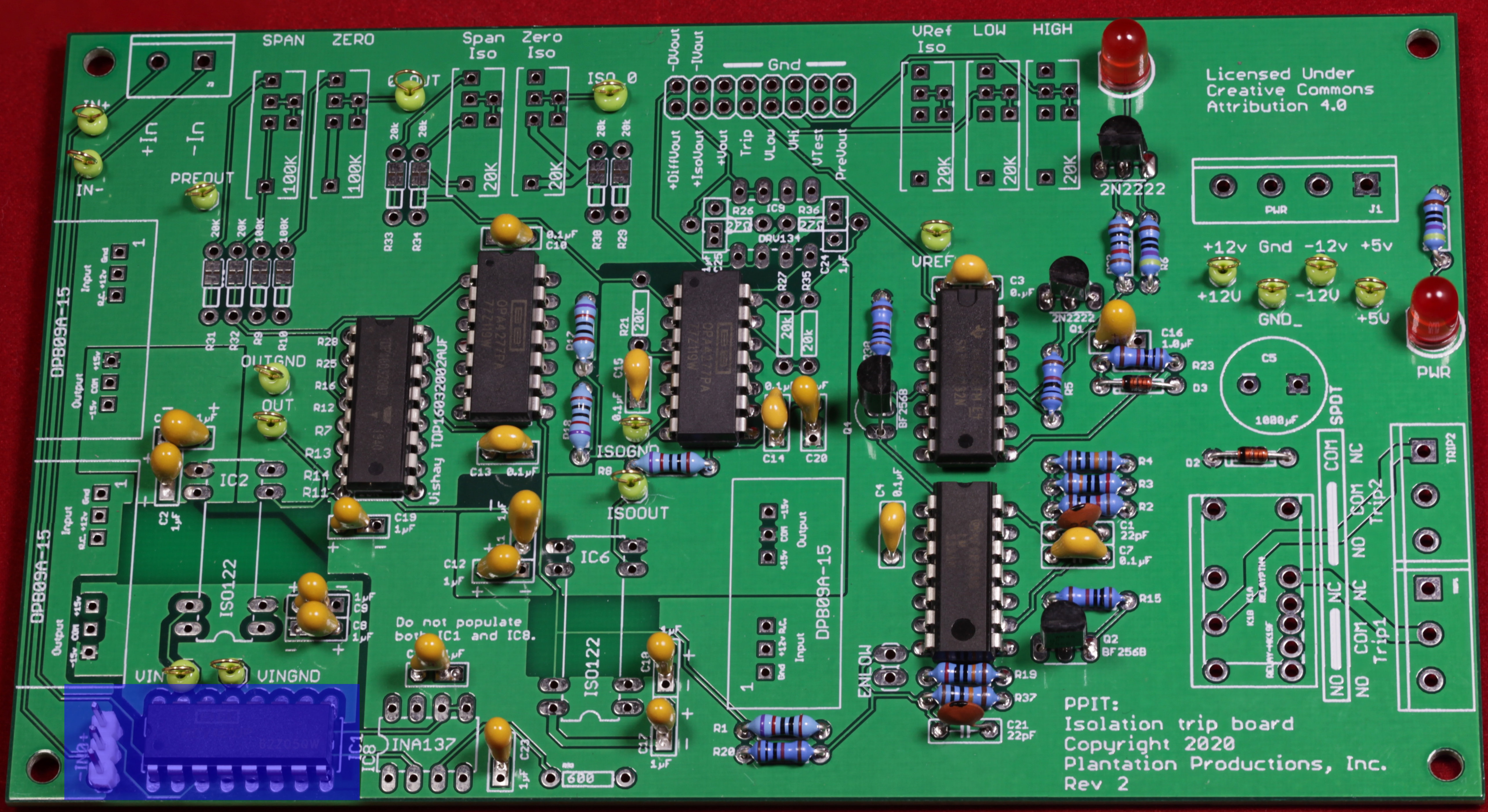
- If you're installing the Vishay array, now is the time to do that. Note that the resistors in the package go from a left pin to a right pin. The array can be installed with the notch up or down, it doesn't matter. I install with the notch up to be consistent with the other ICs on the PCB. If you installed eight discrete 20KΩ resistors in the previous step, skip this step.
High resolution image
- If you're building a board with the differential output driven by the OPA4227 opamp, the next step is to install the two 27Ω 1% metal-film resistors on the board (R26 and R36). These two resistors are a bit hard to find on the PCB as they overlay the DRV134 pins (the DRV134 and its two filter capactors are not installed when building a board with differential output based on the OPA4227). Remember, you must also install R21, R27, and R35 (the 20KΩ resistors) when building the board in this mode. Those resistors are not shown in the picture below because this board is being built for differential output using the DRV134; the 27Ω resistors were inserted on the board in the picture below to show their position, they'll be removed in the next picture.
High resolution image
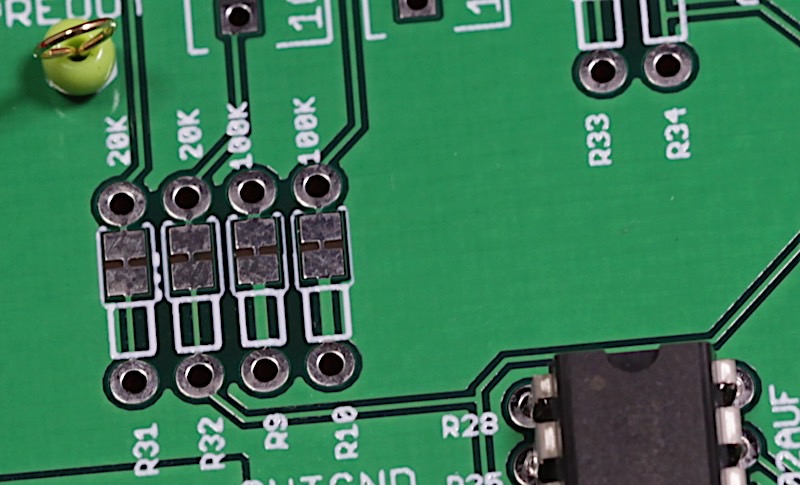
- The last set of resistors are optional. The 20KΩ gain (span) potentiometers on the board will scale from about 0.5 gain (-6dB) to a very high number (pretty much the limits of the OPA4227 opamps). While this is useful, most of the time you only need a gain in the range 0.5 to about 2 (-6db to +6dB). While the wide range on the standard build certainly covers this range, there are two problems with it: (1) initial calibration is tricky when the gain is set very high (which is often the default setting for the pots from the factory); (2) fine adjustment of the gain is very touchy and can be difficult. The solution is to put a resistor on either side of the gain pot to limit the range (and also make the adjustments finer). The PPIT design allows the addition of four 4.7KΩ resistors (one pair on each pot) to reduce the range and allow for finer adjustments.
The same problem exists with the offset (zero) pots. Normally, these pots allow summing a voltage between -15V and +15V to the input signal. Most of the time, you don't need this range–a few volts will work fine. Therefore, the PPIT design also allows the insertion of a pair of 4.7KΩ resistors around the offset (zero) pots to reduce their working range (and allow for somewhat finer adjustments).
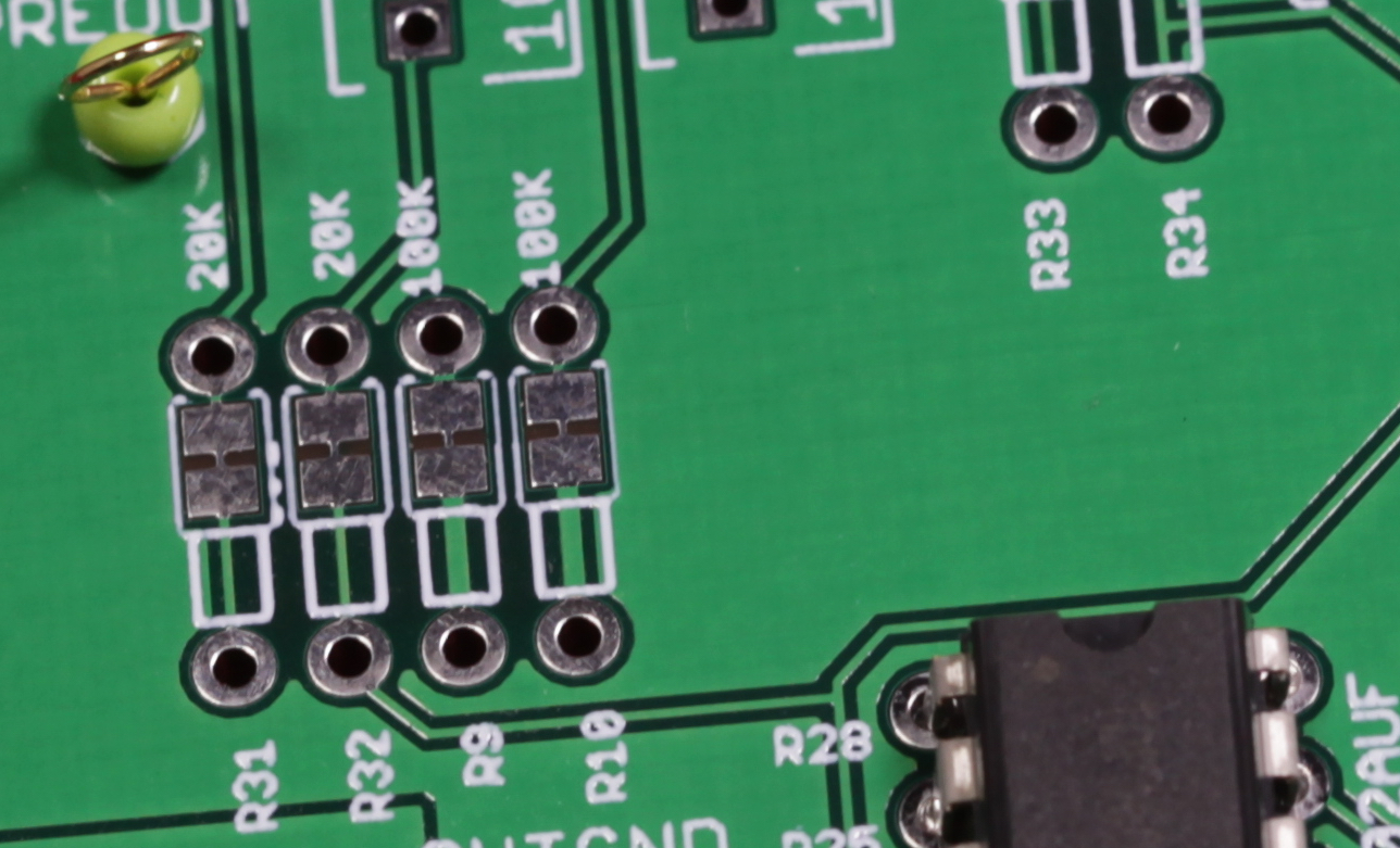
By default, the PPIT design bypasses these resistors (see the picture below). If you want to install these resistors, you will need to cut the traces between solderpads situated between the resistor pins. Resistors R31 and R32 are associated with the gain (span) pot on the normal amplifier circuit. Resistors R33 and R34 are associated with the gain (span) pot on the isolation output circuit. Resistors R9 and R10 are associated with the offset (zero) pot on the standard amplifier and resistors R29 and R30 are associated with the offset (zero) pot on the isolation amplifier output. You may choose to cut the traces and install the resistors on all or none of these pots.
Note: the Rev 2 board lists these resistors as 20KΩ or 100KΩ. They were all changed to 4.7KΩ in Rev 3 (and you should install 4.7KΩ even on Rev 2 boards, if you happen to come across one).
If you accidentally cut one of these traces and decide not to install the resistor (or remove a resistor once you decide you prefer the original design), you can always put a solder bridge across the two pads to reconnect them. Note, however, that solder has a different PPM/C rating than PCB traces, so leaving the traces in place is always the best choice if you're not going to install the resistors.
The board being built in this example will not use these resistors, so the following pictures will not show them installed.
High resolution image
High resolution image
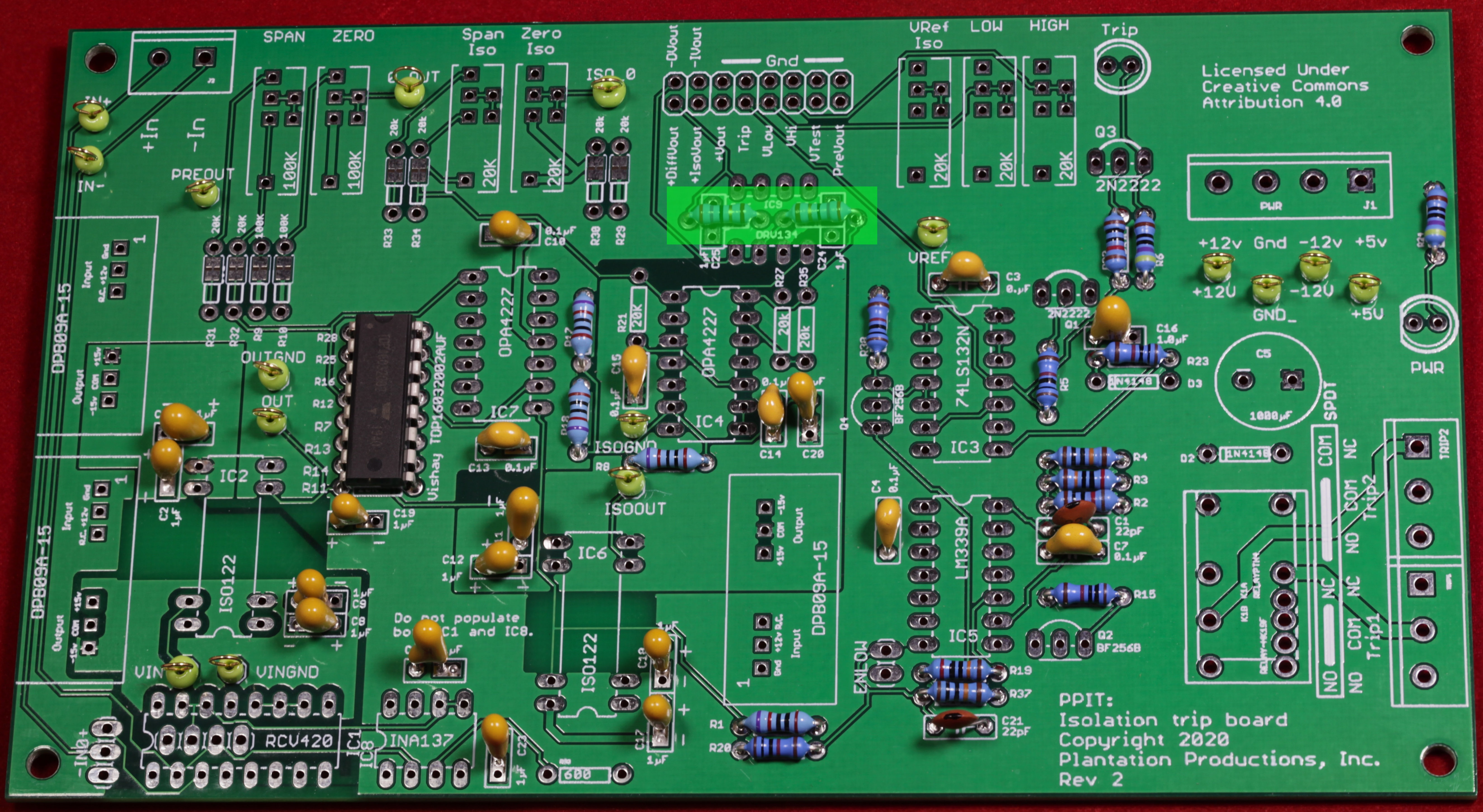
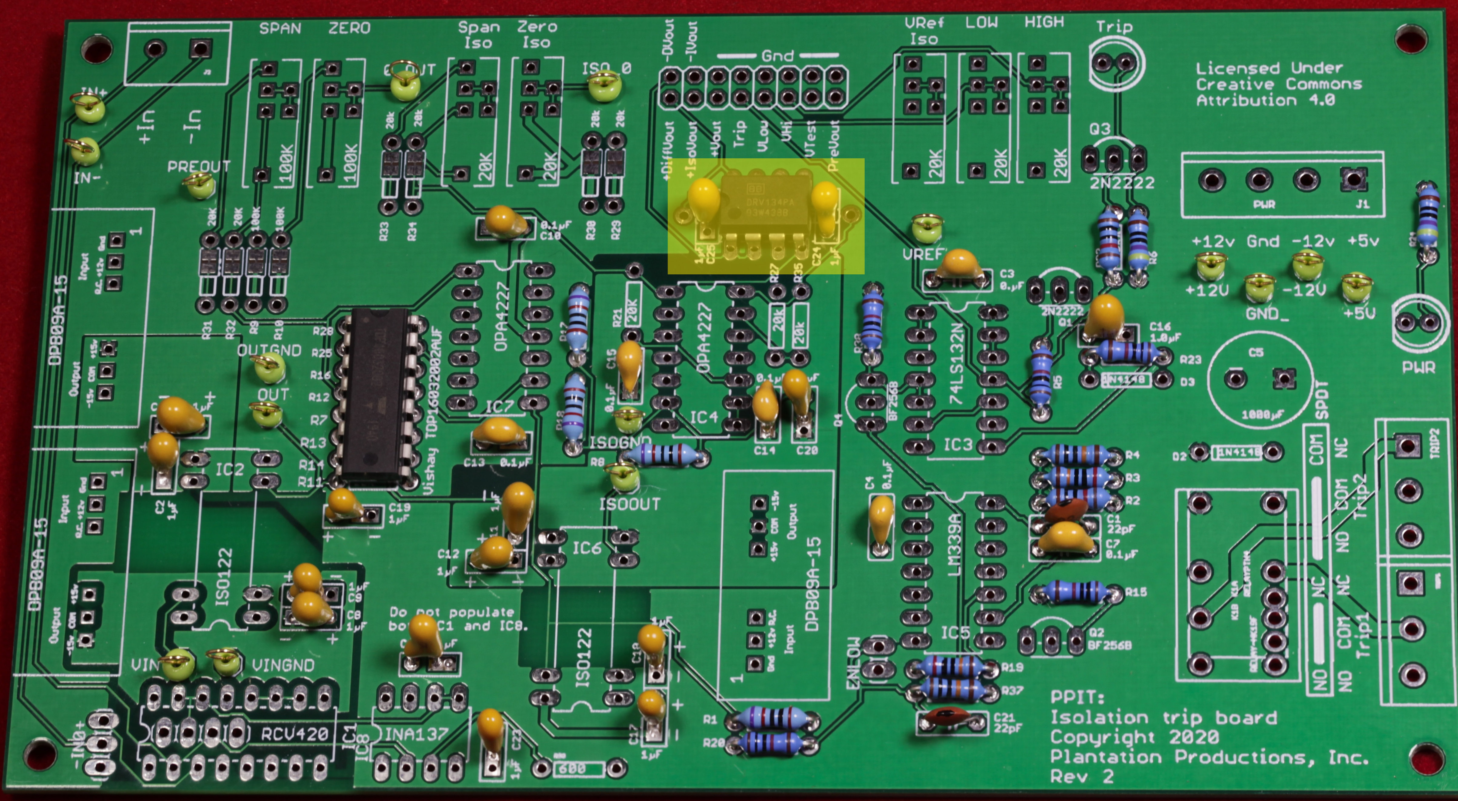
- If you are going to produce differential output using the DRV134 IC, now is the time to install that IC and its two 1µF capacitors.
When inserting ICs, you will notice that the pins on the ICs are actually slanted outward and will not directly fit in the holes on the board (or in holes on the sockets, for that matter). If you have an IC inserter tool, it will automatically bend the pins to the appropriate position prior to insertion. If you don’t have such a tool available, just hold an IC with your fingertips with one row of pins against your workbench or desk and manually bend the pins until they are perpendicular to the body of the IC. Repeat for the pins on the other side of the IC.
Note: avoid the temptation to use sockets for the ICs. Yes, the ICs on this board are not cheap (around $5-$10 each). However, by socketing this ICs you destroy their precision by introducing thermal inaccuracies and noise. If you're going to socket these ICs, you'd be better off using "jellybean" opamps and saving a lot of money (though the accuracy of the circuit will suffer dramatically, see the HDD for details).
IC Insertion Tool:
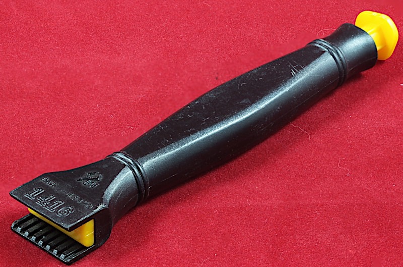
High resolution image
Board with DRV134 soldered directly to the PCB (this is the recommended assembly version). Note that these assembly instructions will show the construction a board that supports single-ended output until the very end. Therefore, the DRV134 IC and its 1µF capacitors will not appear in later pictures in these assembly instructions until the last few pictures.
High resolution image
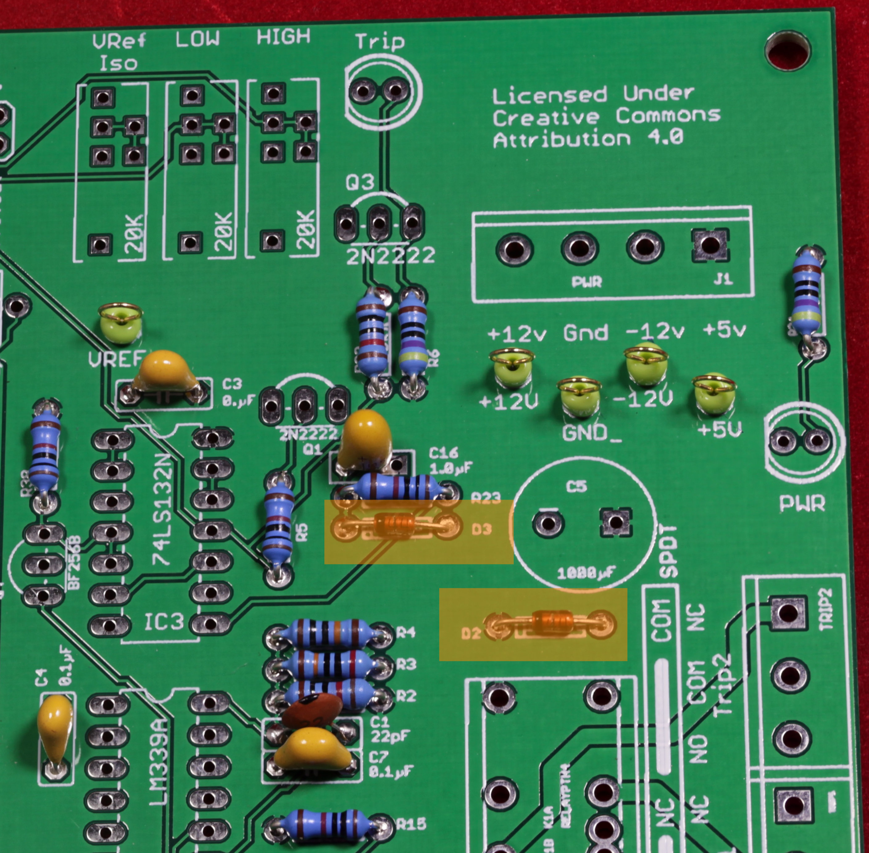
- Next, install the two 1N4148 diodes.
High resolution image
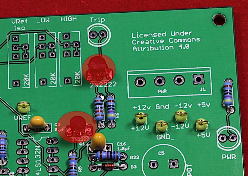
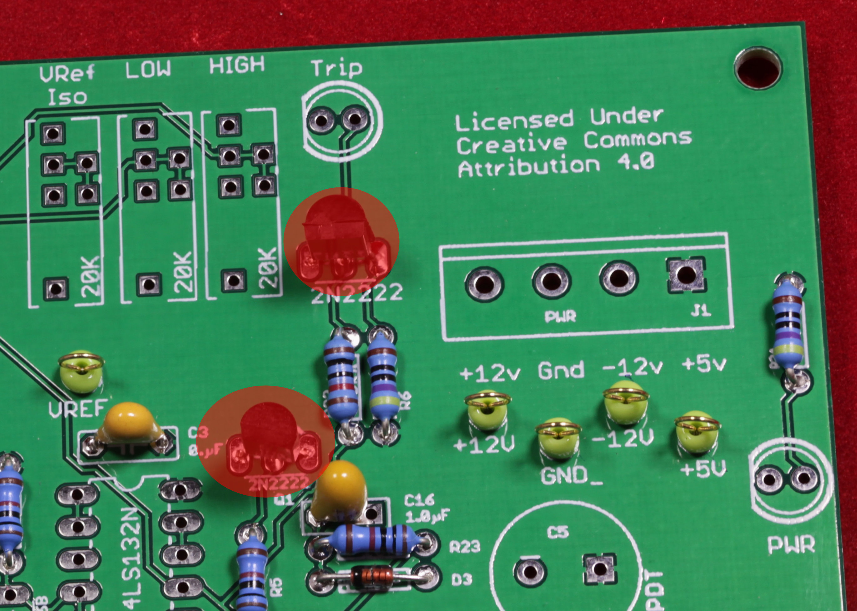
- For the next step, install the two 2N2222 transistors on the PCB.
High resolution image
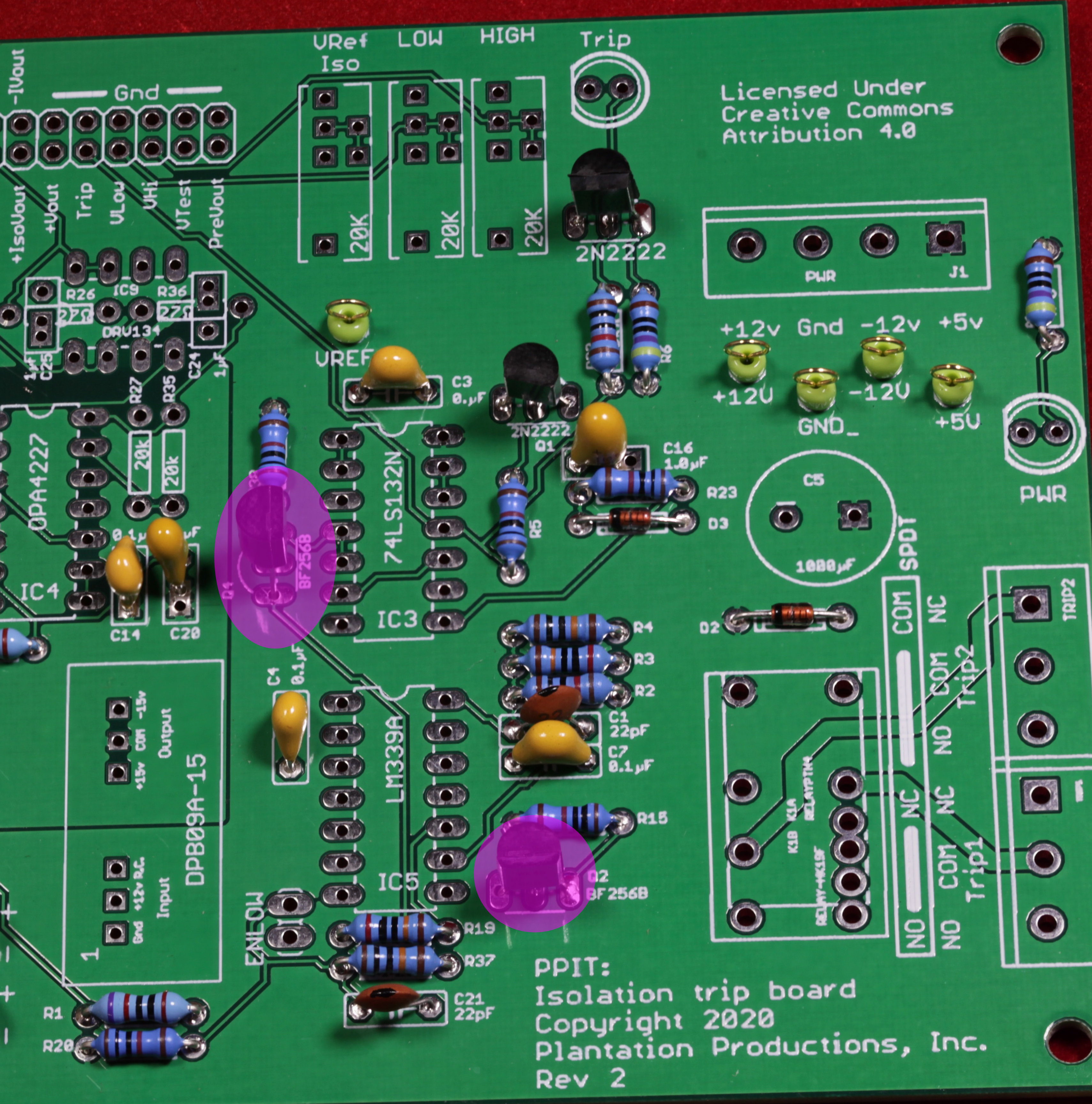
- Now install the two BF256B JEFT transistors on the PCB.
High resolution image
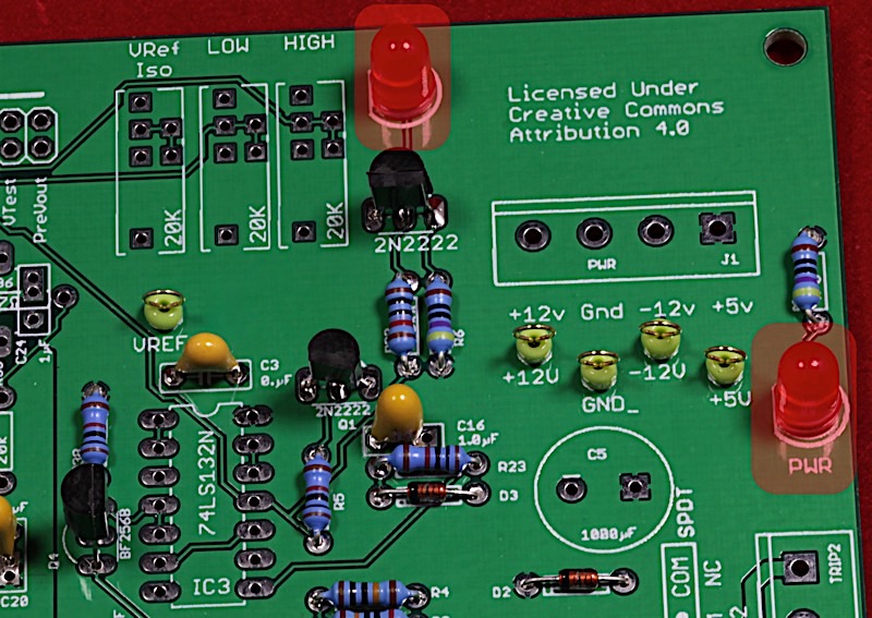
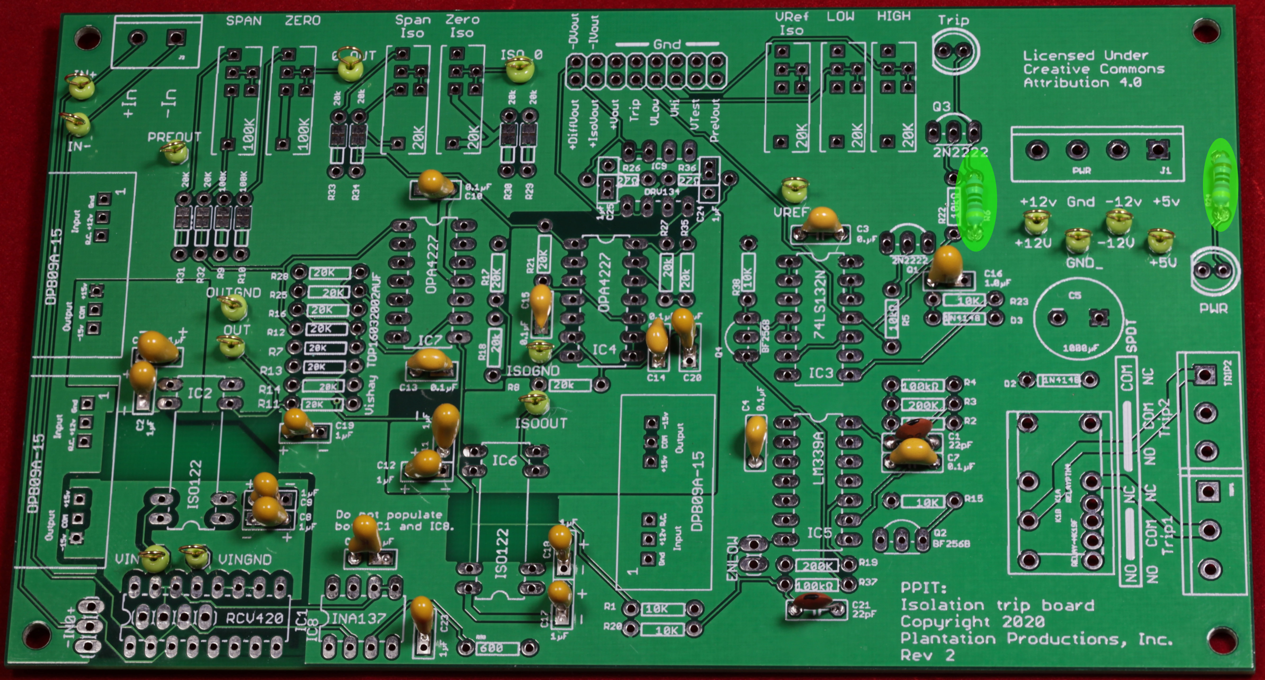
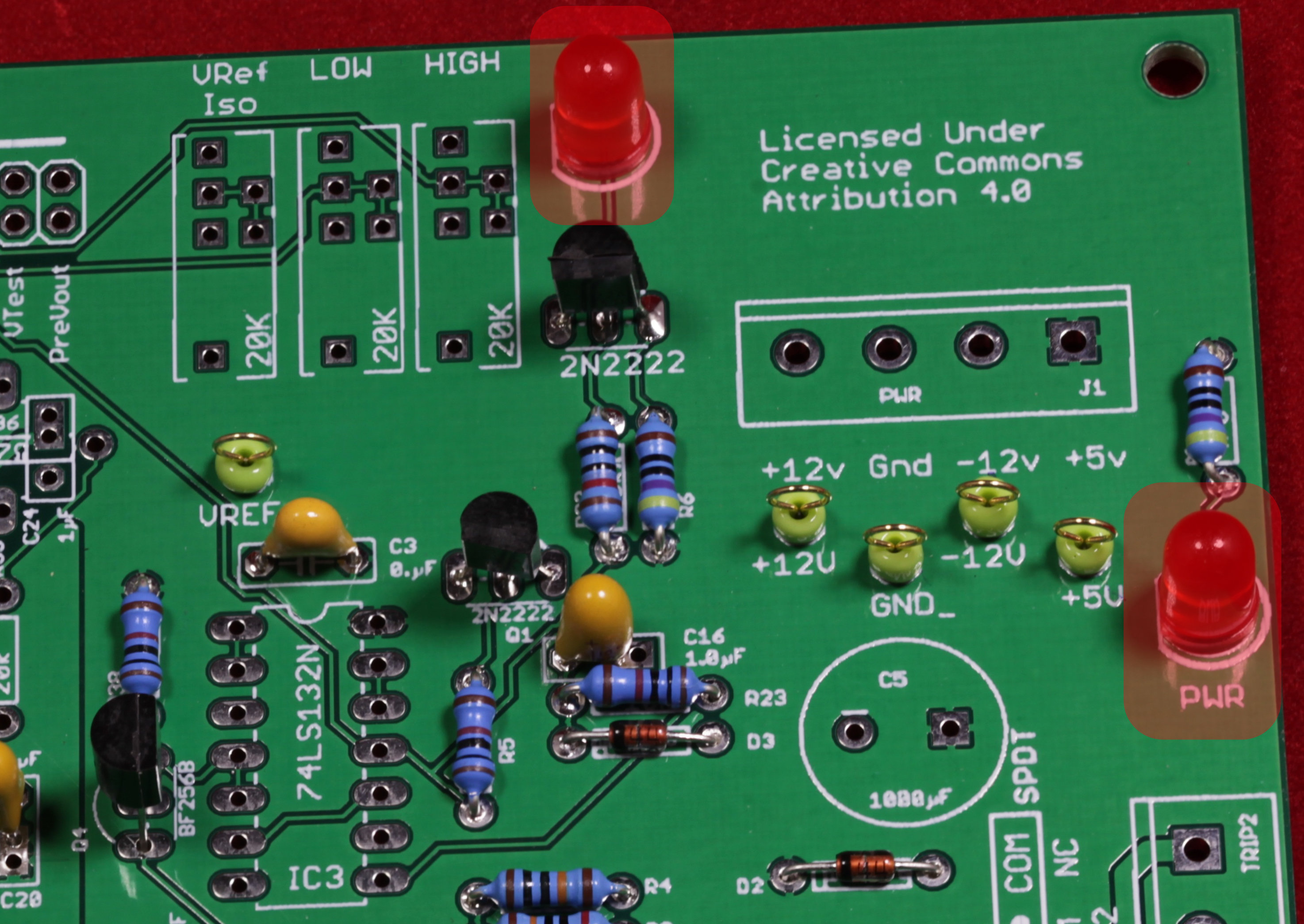
- The next step is to install the two LEDs on the board; remember that LEDs are polarized. The short leg is the negative side and should be soldered to the hole next to the flat side of the silk screen image on the board:
High resolution image
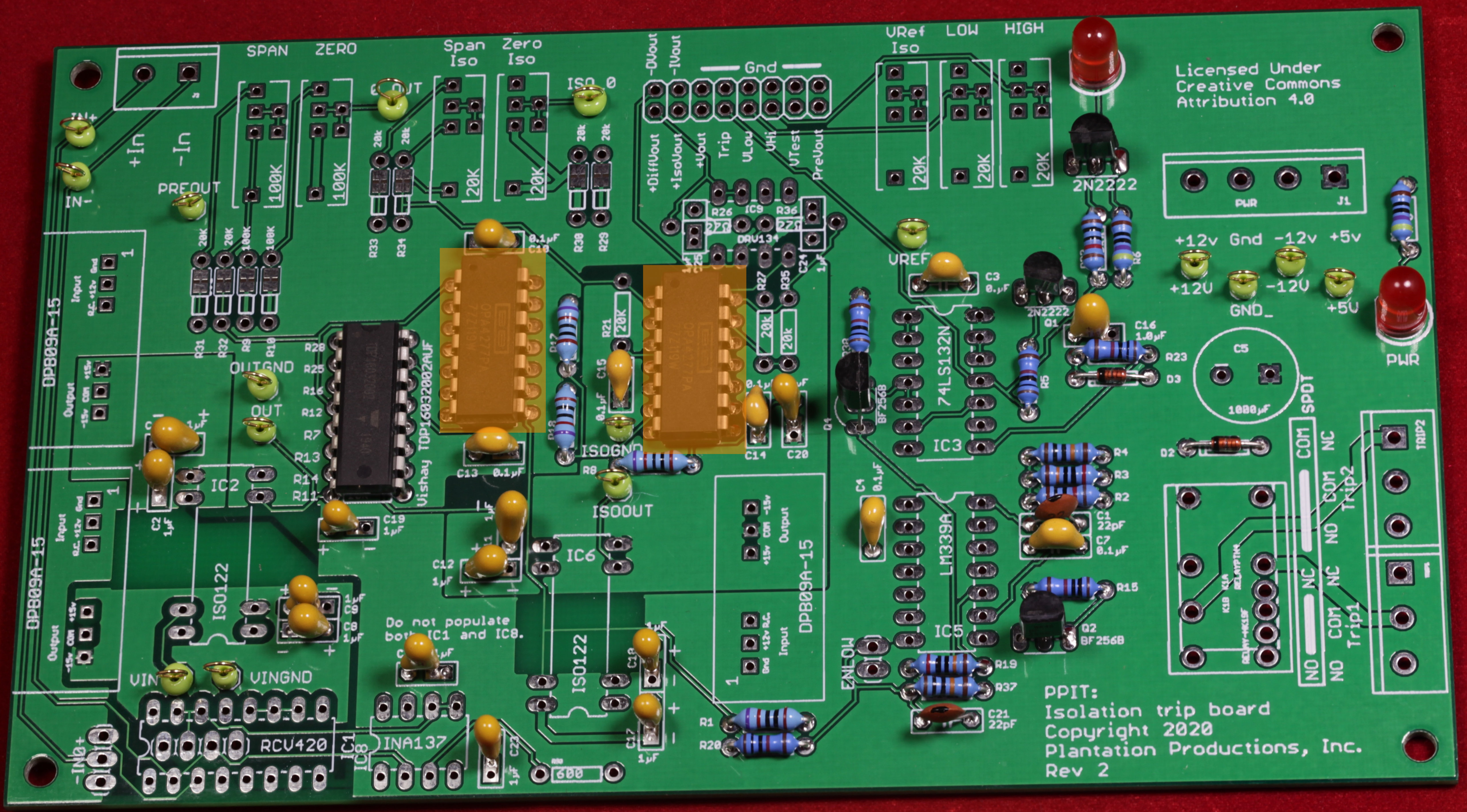
- Now it's time to start installing the ICs on the board. Begin by installing the two OPA4277 opamps. (Note: the Rev 2 board in the picture mislabels these as OPA4227, rest assured, they are really OPA4277 ICs).
Note: if you do not need isolated or differential outputs (+DiffVout/-DVout and +IsoVout/-IVout), you do not need to install the OPA4277 in position IC4.
High resolution image
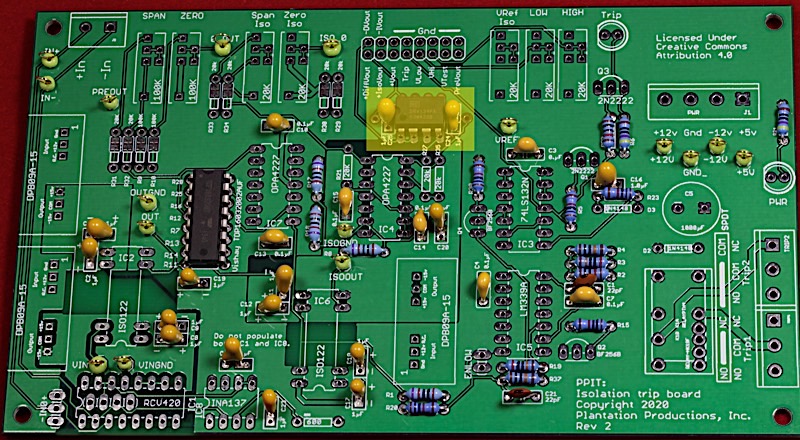
- Install the 74HC132 and LM339A ICs on the board. In the picture below, the 74HC132 is highlighted in white and the LM339A is highlighted in yellow.
High resolution image
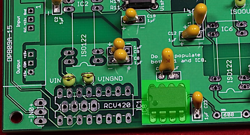
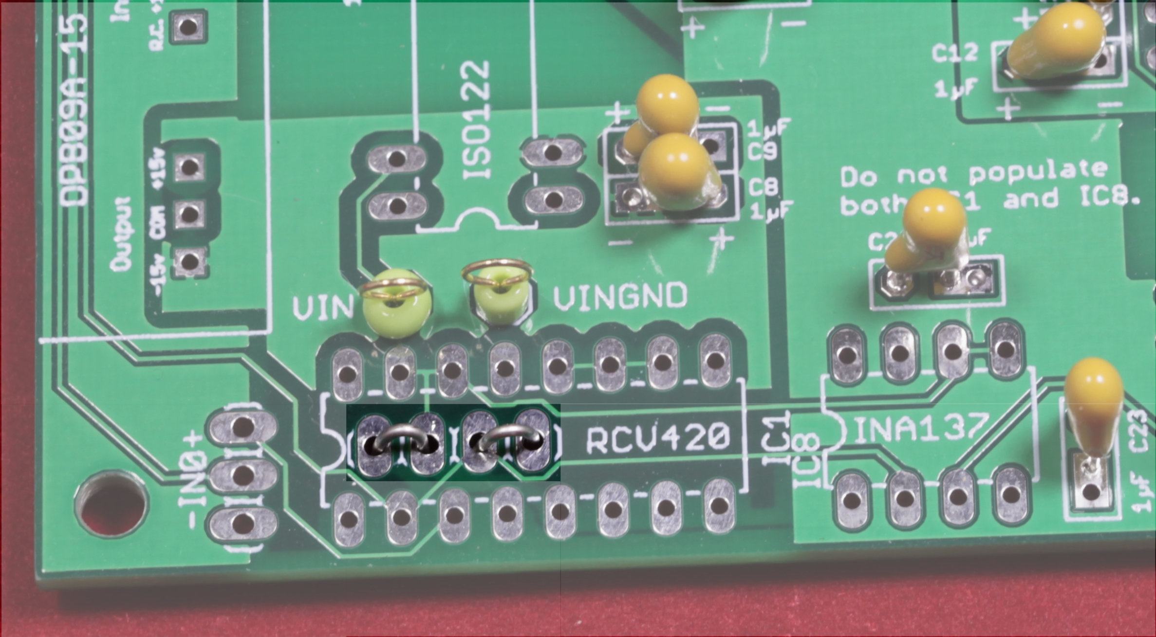
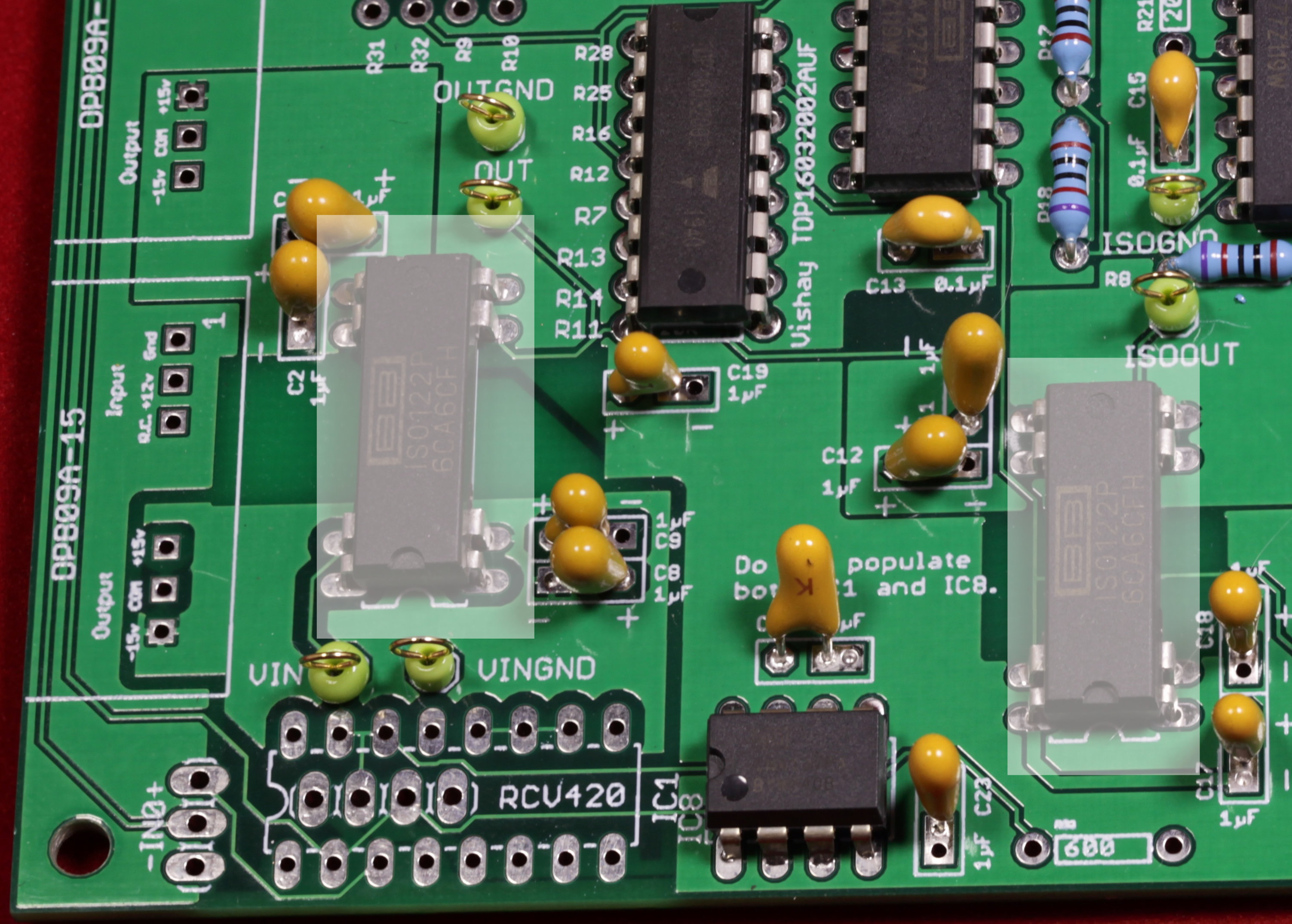
- If you are configuring your PPIT to accept a 4-20mA input, then install an RCV420 IC in the IC1 position as shown in the picture below. Also install a three-pin headerin the three holes labelled -IN0+ (normally, you'd place a jumper between the middle and "+" pins).
Note: when configuring the PPIT for 4-20mA operation, you'd normally not install 1 µF capacitors in positions C22 and C23. They appear in this picture because the board being installed for this example will ultimately accept differential inputs using an INA137 IC.
Also note: leave the IC8 (INA137) holes unpopulated when building a board to accept 4-20mA input.
High resolution image
- If you are configuring your PPIT to accept a single-ended input, then install jumper wires between the two sets of holes inside the IC1 outline as shown in the following diagram.
Note: when configuring the PPIT for single-ended operation, you'd normally not install 1 µF capacitors in positions C22 and C23. They appear in this picture because the board being installed for this example will ultimately accept differential inputs using an INA137 IC.
Also note: leave the IC8 (INA137) holes unpopulated when building a board to accept a single-ended input. Obviously, you must also leave the IC1 holes unpopulated (it would be rather hard, though not impossible, it install the RCV420 over the jump wires). The 3-pin header is not necessary for single-ended operation (it is only used for 4-20mA input).
High resolution image
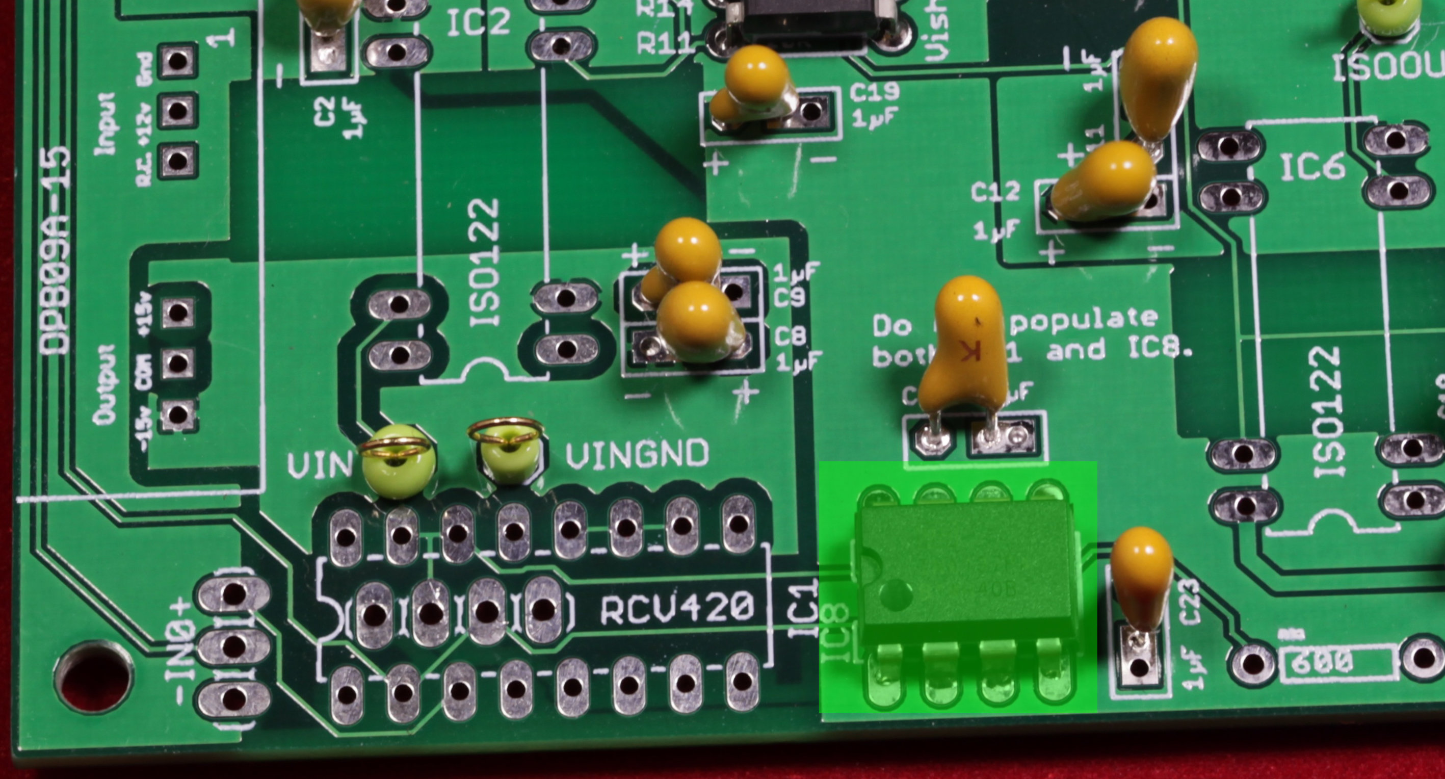
- If you are configuring your PPIT to accept a differential input, then install an INA137 in the IC8 position as shown in the following diagram.
Note: Always leave the IC1 (RCV420) and jumpers under IC1 unoccupied when building a board to accept differential inputs. Likewise, there is no need to populate the 3-pin "-IN0+" header when operating in differential input mode.
High resolution image
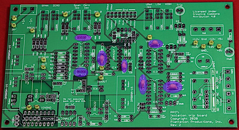
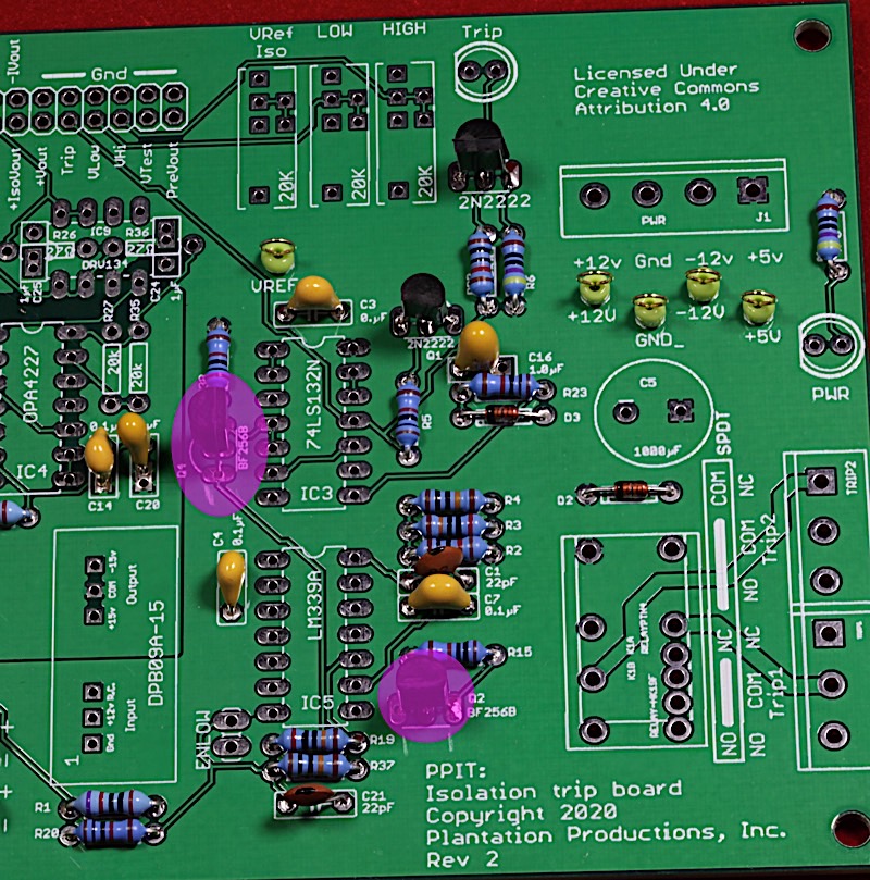
- Next, install the four or five multi-turn potentiometers (two for gain/span, two for offset/zero, and one for Vref).
Note: if you are not implementing the differential/isolated outputs, you do not need to install the pots for ISOSpan and ISOZero (the middle two pots in the picture below). If you are not producing a differential output using the opamp circuit, you do not need to install the VRef Iso pot (which is not installed in the picture below). As these pots are among the most expensive parts on the board, not installing unnecessary pots can save considerable money.
Don't put cheap pots on this board! The pots are the biggest source of drift in the circuit. Using cheap pots (with a high PPM/C value) will easily wipe out the precision of the other parts on the board).
Note that the PCB layout is configured to accept side-slotted pots as well as top-slotted pots. If you elect to use top-slotted pots, be sure to choose pots with a low PPM/C TCR rating.
High resolution image
- The board I'm building during these instructions will have a differential output using the DRV134, so I'll add that IC (and 1µF capacitors) at this time. If you are constructing a board that provides only single-ended outputs, ignore this addition at this point.
The next step is to install the ISO122 isolation amplifier ICs (at IC2 and IC6 positions). Carefully note that these ICs are oriented in the reverse direction of the other ICs on the board (notch towards the bottom of the board rather than the top). This is due to the power supply configuration on the board. Be sure not to install these ICs backwards!
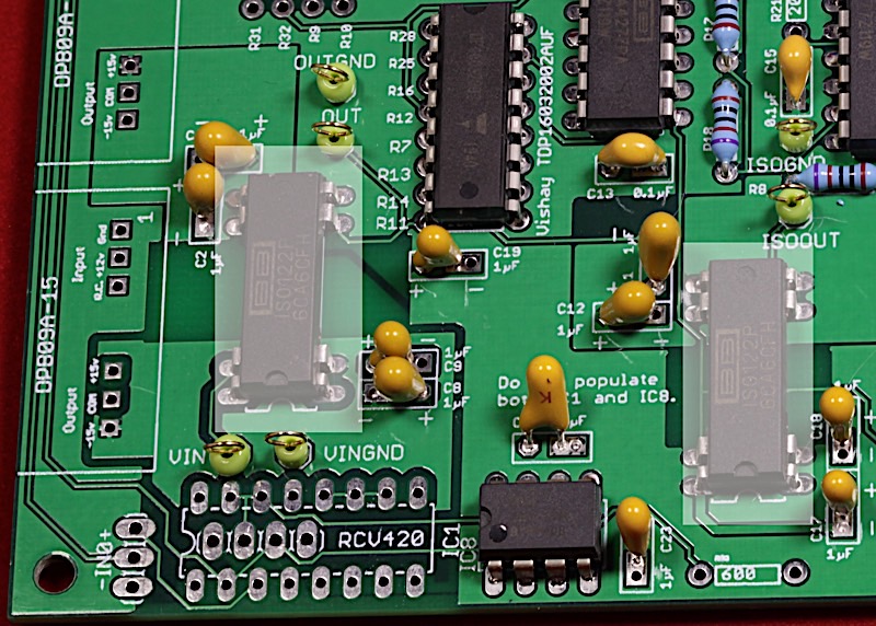
High resolution image
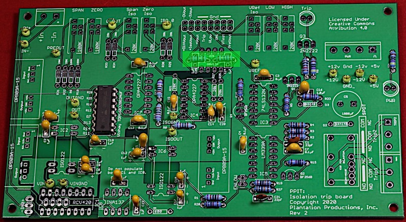
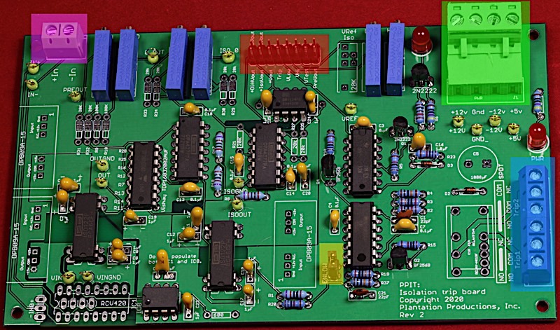
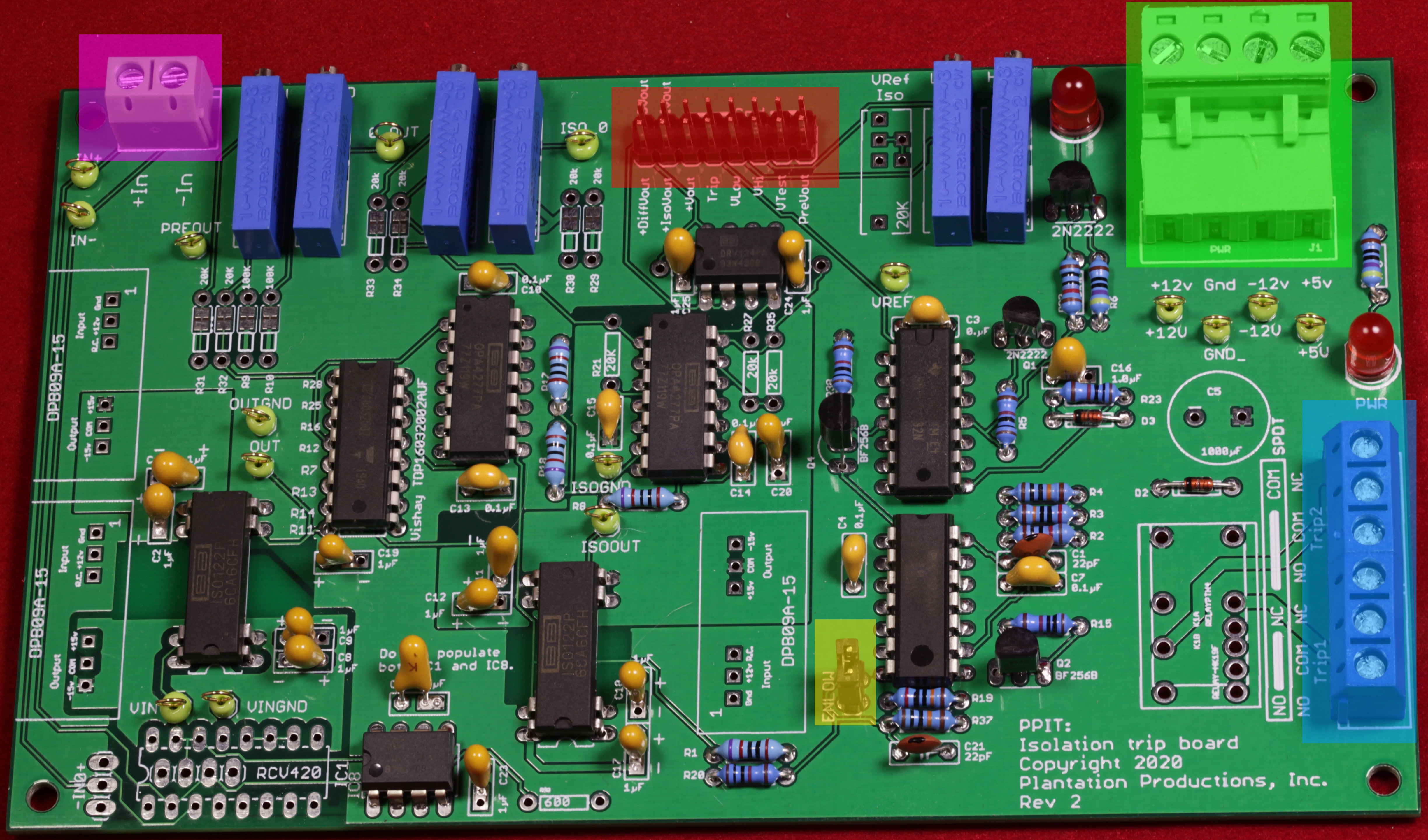
- The next step is to install the 2x8 and 1x2 headers on the board along with the 2-pin screw terminals (for the input signal), the two 3-pin screw terminals (relay contacts), and the 4-pin screw terminals (power supply connector).
The 2-pin header (highlighted in yellow in the picture below) is used to enable or disable the low range of the trip circuit. With a jumper in place (as shown in the picture) the low range is enabled and the comparator circuit will generate a trip if the input voltage is below the VLow set point (set by the "Low" potentiometer). If the jumper is not present, the low range trip is disabled. Note that the high range trip is always enabled. Even if you don't intend to use the low range trip point, put the jumper on at this point because it will be necessary during board testing.
The 2-pin screw terminal (highlighted in magenta in the picture below) contains the connection for the input voltage to this board.
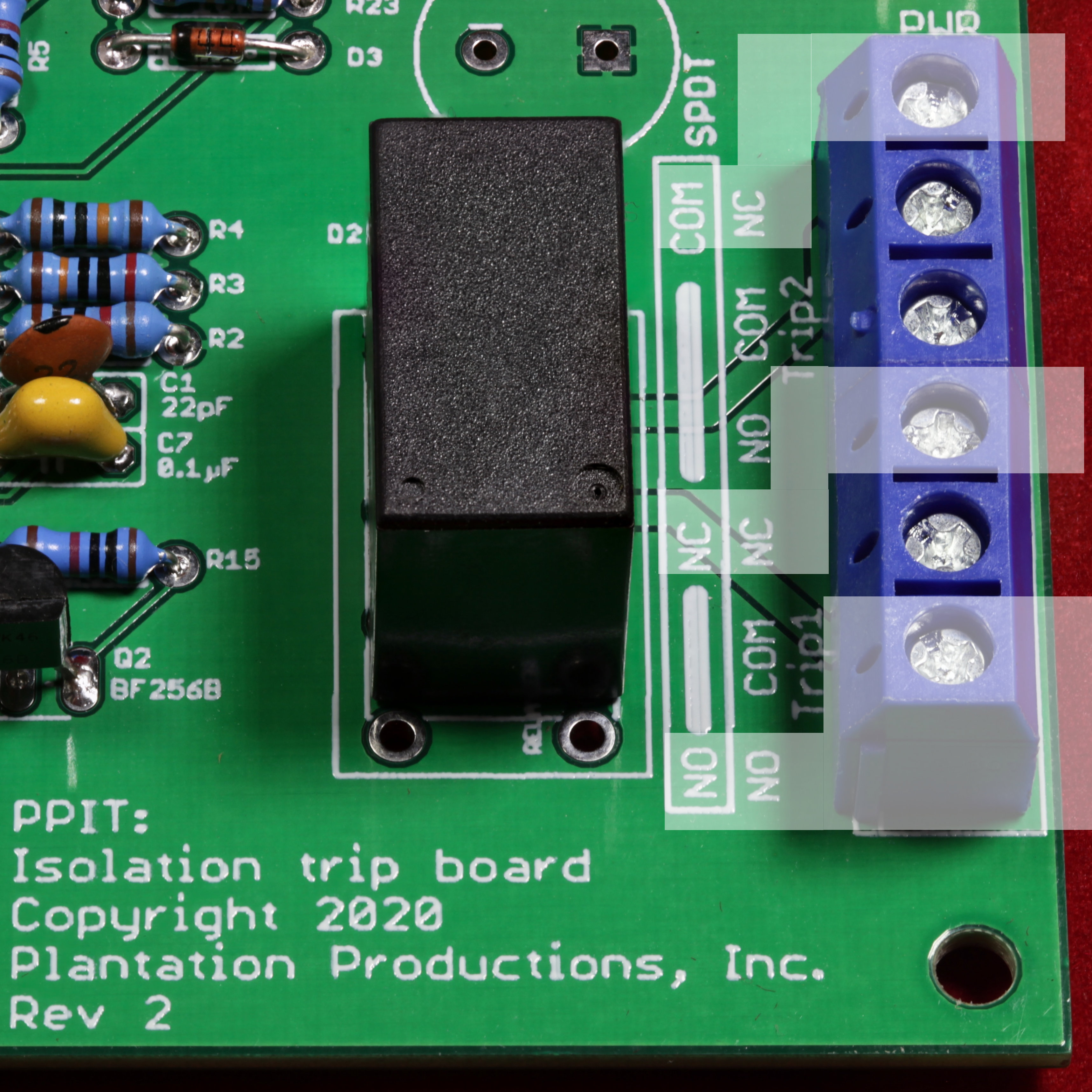
The two 3-pin screw terminals mate to form a 6-pin terminal. When you install a DPDT relay (the
High resolution image
- Now it's time to install the relay. There are two relay choices possible with the PPIT: a SPDT relay (JCZ-11F/005-1Z) or a DPDT relay (HK19F-DC/5V-SHG). The DPDT relay offers two sets of contacts (both switched on/off by the trip circuitry) but are limited to 1A @125VAC or 2A @30VDC. The SPDT relay has only one set of contacts, but can switch 5A at 30VDC or 250VAC.
The picture below shows the DPDT relay installed.
High resolution image
The picture below shows the SPDT relay installed. Note that the two holes closest to the bottom of the PCB are unused by the SPDT relay. Note that the NO (normally open), NC (normally closed), and COM (common) contact connections appear at different locations on the 6-pin screw terminal than for the DPDT relay. This is due to the fact that the two relays share certain hole locations on the PCB but the signals are not the same on these holes. The remaining three pins on the 6-pin terminal strip are "no connections" when an SPDT relay is installed.
High resolution image
- Next, install the 1000 µF capacitor. Electrolytic capacitors are polarized, to be sure to install the capacitor correctly. The negative lead (marked on the capacitor, but also the shorter of the two leads) goes in the round hole (marked with a "-"). This (large) capacitor is used to filter the 5V power supply when the relay switches on or off (which can produce a big surge on the 5V line).
High resolution image
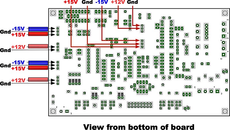
- The last step is to install the three Meanwell DPB09A-15 isolation power supplies. Two of these isolation power supplies are used to produce an isolated ±15V for the ISO122 isolation amplifiers (this isolates the circuitry from the input signal and the isolated output signal). One supply just acts as a bucking power supply to boost the ±12V coming into the board to ±15V (the grounds are connected together on the iso pwr supply, so it's not performing an isolation; the DPB09A-15 was used in this manner to avoid specifying yet another part on the board).
The PPIT runs off ±12V and 5V because these are the standard voltages for the Plantation Productions' DAQ system boards. In fact, you could run ±15V directly to the power connector in place of the ±12V and the board will work just fine. If you do this, there is no reason to install the DPB09A isolation power supply that is being used as a bucking power supply. Instead, you could wire the +12V input to the power supply to the +15V output. You would also run a wire from the -12V power supply connector to the -15V isolated leg of the DPB09A-15 as shown in the following diagram:
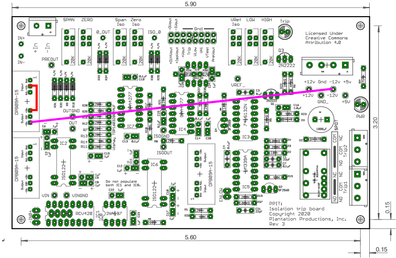
Note that there is no need to connect the grounds together; that has already been done on the PCB.
If you install these two jumper wires, and run the PPIT board off ±15V, you can avoid installing one of the DPB09A-15 power supplies (which are rather expensive components).
Note that the DPB09A-15 isolation power supplies will run just fine off ±15V (they are spec'd to run off 9-18V). So if you don't want to hack up the board but you still want to run off ±15V, you can still install the DPB09A-15 if you like.
Of course, the other two DPB09A-15 power supplies must be installed in order to isolate the input and output signals on the board. The following picture shows the board with all three power supplies installed.
Note: The DPB09A-15 in the middle of the board is installed in an opposite orientation of the other two power supplies. The modules will sit comfortably in the silkscreen outline when they are installed properly.
High resolution image
- At this point, soldering is largely complete (assuming you ’ve made no mistakes that will require some rework). Turn the board over and slowly, careful, visually inspect every solder joint. Well over 50% of the failures I’ve had were due to missing a solder connection (a majority of the remaining failures is installing a polarized capacitor backwards). It’s worthwhile to visually inspect all the pins (yeah, I know, there are a lot of them) to verify you haven’t missed any.
- Now for the actual “smoke” test. With the ICs inserted, apply power and make sure the LED still lights up (no flickering!) and nothing gets overly hot (or worse, smokes and catches on fire! Yes, this has happened to me in the past).
Testing and Calibrating the PPIT Board
To test the PPIT board (assuming you've passed the "smoke" test), the first thing to do is check the voltage outputs from the DPB09A-15 isolation power supplies. Applying voltage (±12V and +5V) to the system, measuring the voltages at the following points on the bottom of the board:
The PPIT board contains two calibration pots for the main and isolation outputs to set the ZERO (offset) and SPAN (gain) values. It also contains two pots to set the high and low trip voltages. For boards that have installed differential output using the opamp circuit, there is a fifth pot to adjust the differential output.
The ZERO pot is useful because the ISO122 isolation amplifier always adds a small voltage offset to the output of the amplifier (that is, if you put in exactly 0V as input to the ISO122 you'll probably not get exactly 0V as the output from the amp -- the ISO122 can add a small negative or positive voltage offset to the input voltage). Also, it's unlike the plus and minus legs of the ±15V power supply are exactly equal in magnitude, so the ZERO pot can help offset for differences there as well as inexact resistor values in the opamp circuits.
The SPAN pot adjusts the overall gain of the opamp circuits (note that a dual opamp circuit follows the isolation amplifier; the isolation amplifier has a gain of 1 which is not adjustable). The PPIT board accepts an input voltage that can range from -10V to +10V input (or a current that can range from 0 mA to 20 mA, producing a voltage in the range -1.25V to +5V) and it can produce an output voltage also in the range -10V to +10V. This does not imply that the output voltage must exactly match the input voltage (i.e., a gain of one). You could, for example, have 0 to 5V input voltage that produces a -10V to +10V output (very typical of processing the output of a digital-to-analog converter). As another example, you could take a -10V to +10V input from the field and produce an output voltage in the range 0 to 3.3V, for use as input to an analog-to-digital converter on a 3.3V microprocessor.
Calibrating the PPIT consists of iterating the following steps for ±10V operation (input and output, with a gain of 1):
- To begin with, attach a variable power supply to the 2-pin input screw terminals and attach DMM leads to the +Vout and Gnd pins on the 2x8 output header.
- Set the variable power supply to 0V and adjust the normal (non-isolation) ZERO pot to produce as close to 0.000V as you can get (you should be able to get within 0.01V to 0.02V without too much difficulty). Note: the standard ZERO pot is the one (labelled ZERO) closest to the input screw terminals.
- Set the varible power supply to +10V and adjust the standard SPAN pot to produce an output voltage as close as possible to +10.000V (you should be able to get within 0.01V to 0.02V of 10V without too much difficulty). Note: the standard SPAN pot is the one (labelled SPAN) closest to the input screw terminals.
- Repeat steps (2) and (3) until you don't have to adjust the ZERO or SPAN pots to get the output voltage within range (often, adjust the SPAN pot will affect the zero setting and adjusting the ZERO pot will affect the maximum output voltage rating; calibration consists of iteratively adjusting the two pots until no further adjustments are necessary and you can switch the input voltage between 0V and 10V and the output tracks the inputs).
- If you are going to operate the PPIT with inputs between -10V and +10V, subsistute -10V for 0V when calibrating the system. (If you don't have a power supply that produces postive and negative voltages, just swap the plus and minus leads on the power supply to get negative voltages.) Note, however, that if you calibrate for -10V (rather than 0V), then a 0V input may produce an output that is slightly less than or greater than 0V (similarly, if you calibrate for 0V, an input of -10V may produce an output that is slightly off). Calibrate to the base voltage (0V or -10V) which is most important to you for the output value.
- If you are operating the PPIT in some other range (besides 0V to 10V or -10V to +10V), you should calibrate the SPAN and ZERO pots using the minimum and maximum ranges you intend to operate on.
Note: If you are using differential inputs, don't forget that the INA137 differential receiver applies a gain factor of -6dB (0.5) to the input. That is, if you input a voltage of 10V between the -In and +In inputs, the output from the INA137 will actually be 5V (gain of 0.5). You can adjust for this by setting the gain of the amplifier stage to 2 (+6dB) to boost the +Vout/Gnd output back up to 10V. Note, however, that if you intend to produce a differential output using the DRV134 differential transmitter, that chip will automatically apply a gain of two (+6dB), counteracting the gain reduction by the INA137. Note, however, that the +Vout/Gnd outputs do not go through the DRV134, so the voltage will be half the input if the gain is set to one. Normally, one circuit transmits a differential signal via the DRV134 to a separate circuit with an INA137, so the gains cancel each other out.
- The PPIT 2x8 header includes two sets of isolated output pins: +DiffVout/-DVout and +IsoVout/-IVout. Both are driven by the second opamp on the PPIT (the differential output can be driven by either a DRV137 or a couple of opamps in the OPA4277 package). As a general rule, you use either the isolation outputs or the differential outputs, you do not use both. The reason is that the calibration is different for both outputs and there is only one set of calibration pots for the isolated outputs. So you can either calibrate the +IsoVout/-IVout outputs or the +DiffVout/-DVout outputs, but not both (calibrating one will mess up the calibration of the other and the two will not be in sync).
- Before calibrating the differential or isolation outputs, you must first be sure that the standard (non-isolated) output is calibrated (as specified in the previous steps).
- To calibrate the isolated outputs you place the DMM probes on the +IsoVout/-IVout pins on the output header. Then follow the calibration procedure given earlier using the IsoSpan and IsoZero pots (the two SPAN/ZERO pots closest to the 2x8 header).
- To calibrate the differential outputs, you place the DMM probes on the +DiffVout/-DVout pins on the 2x8 output header and follow the calibration procedure given earlier except that the maximum voltage will be twice the input voltage (that is, you'll see an output of 20V in response to a 10V input). This is because the DRV137 differential transmitter adds in a gain of two (+6dB). If there is an INA134 receiver at the other end, its gain of 0.5 (-6dB) will cancel out the gain produced by the DRV137. Having a higher voltage on the differential lines reduces noise.
The last thing to test is the trip circuitry on the PPIT board. Earlier, when initializing the pot values, you set the Low voltage set point to something slightly greater than 1.0V and the High voltage set point to something less than 5.0V. With the ENLOW (enable low voltage trip) jumper in place (on the 1x2 header next to the LM339A IC), this means that the trip circuit should produce a trip whenever the voltage is 1.0V or less, or when the input voltage is 5.0V or greater. To verify this, set the input power supply to 1.0V and verify that the TRIP LED is illuminated. Set the input voltage to 2.0V and verify that the LED extinguishes. Then raise it up to 5.0V again, and verify that the TRIP LED comes back on.
Connect the DMM to pins Trip and Gnd on the 2x8 output header. Set the input voltage to 1.0 (or less). Verify that a trip occurs (TRIP LED should be on). Verify that you see a logic zero (0.7V or less) on the Trip output pin. Set the input voltage to 2.0V. Verify that the trip goes away (the TRIP LED should be extinguished). Verify that you see a logic one (3.3V or greater) on the Trip output pin. Raise the input voltage up to 5.0V. Verify that the Trip output remains a logic one (3.3V or greater) until the trip comes in around 5.0V, at which point the Trip pin should register a logic zero (0.7V or less).
Put the DMM on the VLow and Gnd pins on the 2x8 output header. Verify that it registers somewhere around 1.0V (that you set earlier). Put the DMM probes on the VHi and Gnd pins on the 2x8 output header. Verify that it registers somewhat less than 5.0V (as set earlier).
The next test is going to check out the VTest input pin on the 2x8 output header. Put the DMM on the +Vout and Gnd pins on the 2x8 header. Set the input voltage to some value between 2.5V and 3.0V. Verify that you get approximately this value appearing on the +Vout pin. If you have a second variable power supply handy, attach its outputs to the VTest and Gnd pins on the 2x8 output header. With the output set to 0V (on the second power supply), verify that the +Vout output is still registering between 2.5 and 3.0V (as input from the first power supply). Raise the voltage on the VTest pin by 1.0V and verify that the +Vout pin raise to 1V above the value of the first power supply (that is, the +Vout pin is the sum of the VTest and input pins). Raise the voltage on the VTest pin by 2.5 to 3.0V. Verify the +Vout pin outputs the sum of the two voltage and the TRIP occurs.
Note: if you don't have a second variable power supply available, a 5V power supply will work, or you can just run leads from the first power supply to the +Vout and VTest pin and expect to see a doubled voltage on the +Vout pin.
Move the DMM probes to the PreVout and Gnd pins on the 2x8 header (leave the second power supply hooked up). Set the second power supply to 0V. Verify that the voltage on the PreVout pin matches the input voltage (from the first power supply). Raise the voltage on the second power supply (to the point you get a trip). Verify that the PreVout pin voltage does not change.
Note: PreVout is the +Vout voltage without the summation of the VTest input voltage. This pin allows you to continue to monitor the actual input voltage while applying a test voltage to the VTest pin.
Disconnect the second power supply (we're through with it).
Set the input voltage to 1.0V (this should produce a trip). Using the DMM, measure the resistance between the COM and NC pins on the relay. They should be shorted together (low ohmage). Measure the resistance of the COM and NO pins; they should be open (infinite resistance).
Note: if you've installed the DPDT relay, measure the resistance of both COM/NC terminals and verify that both contacts are closed. Likewise, verify both sets of COM/NO contacts are open.
Set the input voltage to 2.0V (which should clear the trip). Measure the resistance of the COM/NC contacts; they should be open (high resistance); also the COM/NO contacts should be closed (low resistance).
Assuming all of the above tests pass, your PPIT board should be working properly.
Hardware Design Description
The PPIT board was designed to implement three separate functions from the Plantation Productions' PPDAQ series into a single board: analog input isolation and amplification (plus conversion from 4-20mA or differential inputs, if necessary), an analog trip circuit, and an output isolation amplifier (also supporting differential output). Previously, this could be accomplished using two PPISO4 boards (with appropriate daughter boards for current loop and differential I/O) and a PPAT4 board, to achieve four channels. However, the major use case for the PPIT (the nuclear fuel temperature monitor, or FTM) only requires three channels and doesn't require many of the features on the PPISO4 and PPAT4 boards. Furthermore, the PPAT4's design tended to use jellybean components, so drift was a bit of a problem So the PPIT board was designed to specifically handle the needs of the FTM.
The main goal of the PPIT design was to produce a board that, once calibrated, would hold that calibration for a reasonable length of time (i.e., no more than a couple calibrations per year, at most). Fundamentally, this meant disposing with the jellybean parts (e.g., $0.50 for an LM324 opamp, $1.50 for a trim pot, and a few cents each for 1% resistors) and designing the PPISO4 using instrumentation-quality opamps and resistors. Instrumentation-quality opamps are 10x to 20x more expensive than jellybean opamps (e.g., OPA4277 quad opamps are about $10 each [qty 10] while LM324 quad opamps are about $0.37 each [qty 10] from Mouser Electronics). Whereas cheap 1% metal-film resistors are a couple cents each, precise, low TCR, resistors range from about 10x that amount ($0.25 each) to as much as $5.00 ([or more) depending on how precise you want them. Potentiometers are just as bad. Rather than $0.50 to $1.50 for a typical trim pot, quality pots (with nowhere near the precision or TCR rating of individual resistors) run anywhere from $15.00 to $50.00 for "just good enough." Really, really, good pots can actually cost hundreds of dollars each (too rich for this design!).
When choosing the parts of the PPIT design, reducing output drift (given a stable input) was one of the primary goals. For opamps, the primary features were:
- High CMRR value
- Low input bias current
- Low offset voltage
- Low noise
- Wide power supply range (at least ±18V to handle the ±15V required by the PPIT).
For resistors and pots, the main characteristic to consider was the thermal coefficient of resistance (TCR). This parameter determines how much the resistance will change as a function of temperature. Resistance precision was a secondary concern for individual resistors (not as much for potentiometers).
The TCR rating is especially important for combating drift. Consider the following opamp circuit in the original PPAC4 design:
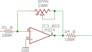
This is a very typical inverting opamp design. The gain is given by -Rfeedback/Rinput (-RSpan/R1_0). Adjusting the pot changes this ratio and, therefore, adjusts the opamp gain. In this particular schematic, the gain ranges from 0 (when RSpan = 0) to -0.5 (when RSpan = 100kΩ). The gain is negative because this is an inverting opamp.
Suppose the pot was set to 50kΩ and left there. As the system (and environment warms up), the resistors' values change. The TCR rating (typically given as PPM/C) defines how much the resistance changes with varying temperatures. Crappy (jellybean) resistors have TCR ratings in the high hundreds (even thousands). Assuming the two resistors (R1_0 and the SPAN pot) changed their resistance in an identical fashion with respect to temperature, this wouldn't be too big of a deal: it's the ratio of the resistance that is important, not the actual resistance values. If the two resistors' values changed (on a percentage basis) in lockstep with the temperature, the ratio would remain fairly constant and the gain wouldn't change that much.
Unfortunately, two different resistors aren't going to have the same exact TCR and, in fact, pots usually have far worse TCR ratings than individual resistors. Therefore, as the temperature changes, the two different resistors will change values at different rates. This will cause the ratio of the resistances to change and, therefore, the gain will change. This will cause the output voltage to drift even though the input voltage remains stable.
The first solution is to choose better resistors (ones with a low[er] TCR rating). For the most part, that's easy enough to do. All it takes is to throw some money at the problem. For example, in quantity one, Mouser Electronics lists a 10kΩ resistor with a TCR between 350 and 500 for around $0.10. Of course, go to Amazon and you can find 100 of them for around six bucks (though no TCR is given, assume it's bad). Indeed, if you buy 1,000 of them on Amazon, you can find carbon-film resistors for around $0.01 each.
Go to Mouser and search for 10kΩ, 15 PPM, 0.1% resistors. You'll find they cost about $0.51 each in quantity 1 ($0.274 each in qty 100). So spending 50 cents each (or a little more than a quarter each, if you buy them in 100 quantity), you'll get much better stability in the circuit.
Can we do better? Sure. How much money do you want to spend? Mouser lists a 10kΩ, 0.01%, 5 PPM/C resistor for only $13.06 (qty 1, qty 100 is $10.05). Do you want to spend over $117 dollars just for the resistors on your PPIT board? I didn't think so. Actually, there's a very pratical reason for not getting resistors that precise–the PCB has its own TCR rating which will be higher than 5 PPM/C. The weakest link in this case is the PCB, so there's really no reason for spending money on high-precision, low-TCR, resistors; the thermal drift from the other components on the board will completely swamp the accuracy of the resistors.
The other issue is the potentiometers on the PPIT board. Although you can get very low TCR, highly precise resistors (if you're willing to pay for them), pots are another issue altogether. Decent pots are 50 PPM/C at 10% accuracy. Such pots cost $15.00 and go way up depending on the resistance. You're also very limited in the resistances you can get; for example, you won't find a low-TCR pot at 100KΩ (at least, not without spending a huge fortune on the pot.
The PPIT specifies 20kΩ pots for the Span and Zero pots. As it turns out, Mouser has 20kΩ pots (50 PPM/C at 10%) but they cost more than 10kΩ parts. When used as voltage dividers, the resistance doesn't matter too much (as long as too much current doesn't flow through the whole pot). So I commonly swap out 10kΩ pots for the 20kΩ pots when building boards.
Here's the schematic for one amplifier section similar to the ones found on the PPIT:
I'll discuss the second stage of the amplifier in a bit. For now, consider the first stage (opamp IC3B, R6_0, R4_0, R5_0, and the Zero0 pot). The input resistor is 10kΩ as is the feedback resistor. Therefore, this stage provides (roughly) unity gain for the input signal (well, -1 gain as it is an inverting amplifier). This is an inverting summing amplifier, adding the input voltage plus 1/2 the voltage coming out of the Zero0 pot (1/2 of this voltage because R4_0 is twice the resistance of R5_0). Because the Zero0 pot divides the voltage between -12V and +12V, this stage of the amplifier can add ±6V to the input signal.
Of course, R4_0 could also be a 10kΩ resistor. In that case, the Zero0 pot would be able to add ±12V to the input signal (though, technically, the PPIT circuit is rated for handling ±10V). However, in real-world situations, most voltage offsets added by a Zero pot are limited to plus or minus a couple of volts. So there really is no reason to allow the full scale ±12V to be added to the input voltage. Cutting the offset voltage in half has one desireable effect: you have to turn the pot twice as many turns to sum in the same voltage as you would if R4_0 had been 10kΩ. This means it's easier to "zero out" the circuit with a fair amount of precision.
If 20kΩ is good, why not go to 40kΩ and make the Zero0 pot even more precise? If you can guarantee you never need more than ±3V for the offset adjustment, this would make sense. However, some ADCs out there don't like negative voltages. So to convert a negative input voltage (say -5V to +5V) to a positive range, you might need to add more than 3V to the input. 20kΩ seemed like a good starting point for the design. However, you can replace this resistor with a larger (or smaller) value depending on your particular requirements.
As for the older PPAC4 design, the R5_0/d R4_0 (input) and R6_0 (feedback) resistors determine the gain of this circuit based on their ratio. When the temperature changes the gain will vary if the resistors' ratio doesn't remain constant. Low TCR (e.g., 15 PPM/C) help prevent the gain from varying too much when the temperature changes.
Note that the resistors' precision (typically 0.1% for these resistors) means that the ratio will be very close to the calculated numbers. That is, ignoring the Zero0 pot sum value (assume it's 0V), the gain will be very close to unity (within the 0.1% tolerance of the resistors).
Pots are a different problem. First of all, the TCR values for pots are usually much higher than for discrete resistors (e.g., 50 PPM/C for the pots specified for the PPIT, versus 15 PPM/C for the discrete resistors). Fortunately, the Zero0 pot is simply a voltage divider. It's value does not directly affect the gain of the opamp stage. Now the voltage divider could have issues if the resistance on one side of the pot's wiper changes with respect to the resistance on the other side of the wiper. However, as the pot is all one unit, the temperature is going to be relatively stable across the whole device and the whole device's resistance will change together. As a result, the effective TCR of the "two" resistors making up the voltage divider is very low (indeed, the wiper probably contributes more to the TCR variance than the actual pot material does).
Now consider the second stage of the amplifer in the circuit given above. This consists of two optional discrete resistors and a pot acting as a voltage divider. This is a big design change from the PPAC4. Look back at the PPAC4 amplifier circuit: The R1_0 and SPAN pot form a voltage divider (with one side of the divider having a fixed resistance and the other side having a variable resistance). As noted before, as the temperature changes, the resistances of the two halves of this voltage divider change by differing amounts, resulting in a gain that drifts with temperature.
Note look at the second stage of the PPIT circuit. The input and feedback resistors are both incorporated into the SPAN0 pot. That is, the left side of the pot (in the schematic diagram) is the input resistor and the portion of the pot to the right of the wiper is the feedback resistor. By combining the two resistors into a single pot, a fair amount of problems with thermal drift go away. Using a decent quality pot (50 PPM/C and 10% tolerance) produces a very stable design.
There is one problem with the voltage divider (PPIT) version versus the two-resistor/variable resistor version (PPPAC4): linearity. The voltage divider in the PPAC4 circuit (with one side fixed and the other variable) produces a linear change in gain as you move the pot wiper from one end to the other. In the PPIT design, moving the pot wiper changes both the input and feedback resistor simultaneously. This produces a very non-linear plot of gain versus pot position, especially as the pot wiper moves to the point the input resistor is zero:
As it turns out, this circuit produces reasonable results between the 20% and 80% positions:
The optional 5kΩ resistors (4.7KΩ in real life) help solve this problem by flattening the curve a bit. They also make the SPAN pot adjustment a little more precise (similar to increasing the size of the resistor on the ZERO pot). HOWEVER, there is a big issue with adding these two resistors: you've now got three different resistors (each with their own TCR) in the circuit. This will (slightly) increase the gain drift. Furthermore, adding additional solder connections affects the overall TCR of the PCB and circuit. So adding the two 5kΩ resistors will flatten the gain curve and make it easier to adjust the gain during calibration, but at the expense of some additional drift. Another issue with adding these resistors is that they limit the maximum gain of the circuit (fixable by using smaller resistors, but that unflattens the curve a bit and makes adjustment a little more difficult). Bottom line is that you should only add these resistors if they are absolutely necessary; they may create more problems than they are worth.
If you decide to add the resistors, note that the default assumption on the PPIT PCB is that they will not be installed. Underneath the resistor positions are some solder pads with traces you must cut before installing these resistors:
4.7kΩ is a good value if you're using 20kΩ SPAN pots. If you're using 10kΩ SPAN pots, 2kΩ would probably be a better choice for these resistors.
The following table lists the range of possible gain and offset values for the pots with and without the limiting resistors installed.
| Pot Value | Limiting Resistor | Gain Range | Offset Range |
|---|---|---|---|
| 10KΩ | Not Installed | 0 to infinity (*) | ±12V |
| 10KΩ | 4.7KΩ | approx 0.32 to 3.12 | approx ±6.2V |
| 10KΩ | 2KΩ | approx 0.17 to 6 | approx ±7.9V |
| 20KΩ | Not Installed | 0 to infinity (*) | ±12V |
| 20KΩ | 4.7KΩ | approx 0.2 to 5.2 | approx ±7.9V |
| 20KΩ | 2KΩ | approx 0.09 to 11 | approx ±10V |
(*) Of course, in the real world you won't actually achieve a range of 0 to infinity. The opamp has physical/electrical limitations that limit the gain to a factor of several hundred or thousand. Also, even if the limiting resistors are not installed, the PCB traces add some resistance (perhaps several hundred milliohms) that prevent these extremes from being reached, even in a theoretical sense.
Note that the higher the range, the less fine (precise) potentiometer adjustments will be; conversely, the lower the range, the finer the adjustments will be.
If you don't install these optional resistors, you should manually measure the SPAN pots before attempting to calibrate the PPIT board. Adjust them to the half-way point (e.g., 10kΩ for a 20kΩ pot, or 5kΩ for a 10kΩ pot). This will ensure that you're not operating at the "crazy" end of the gain curve (from which it's very difficult to begin the calibration process).
Comparator Design
The comparator circuit using a standard LM339A dual comparator IC (a "jellybean" device, though it is very precise). Each comparator in this IC compares the two analog signals appearing on the (+) and (-) inputs and pulls the output low (open-collector output) when the (+) voltage is higher than the (-) voltage.
The PPIT uses 1/2 of the LM339A to test for the high range (when COMPIN, which is +Vout) is higher than the High set point and the other half of the LM339A to test for when COMPIN is less than the Low set point. However, the way the circuit is actually designed can be somewhat confusing at first glance. Note that the COMPIN is connected to the (-) input (pin 8) with the HIGH voltage set pot connected to the (+) input (pin 9). Therefore, this comparator actually pulls its output low when COMPIN is less than the high set point. This contradiction is resolved by the BF256B JFET transistor connected to the output of the comparator (which inverts the signal). Why this craziness? The answer will appear later in this explanation. For now, just accept the fact that the output from the BF256B JFET produces exactly the signal we want — the output gets pulled low when COMPIN is greater than the voltage from the High set point potentiometer
The low-range comparator is largely the same with two exceptions: first, as you would expect, the inputs to the comparator are swapped so that the output gets pulled low on the opposite condition (that is, when COMPIN is less than the voltage output from the Low set point potentiometer). The second difference is the presence of the ENLOW jumper. When shorted, this circuit behaves like its high-set point counterpart. When open, the low set point comparison is removed from the circuit (the 10KΩ pullup resistor following the ENLOW jumper always pulls this signal high, so it's as though the input is never lower than the set point and the trip never occurs). Other than that, the two halves of the LM339A behave the same, with one half pulling the trip output low when COMPIN is greater than the high set point and the other half pulling the trip low when COMPIN is less than the low set point.
By the way, the reason for the double inversion was to correct some problems that would have occurred with the ENLOW circuit.
Also note R3 and R19 in this circuit. Consider R3. When COMPIN is less than the high set point voltage (no trip), pin 14 is high impedance. Therefore, Vcc (+5V) is summed into the (+) input of the comparator (effectively raising the comparison voltage by about 0.2V). So COMPIN actually has to be about 0.2V higher in order to cause an actual trip. This might seem like a disaster waiting to happen (the circuit is not responding to the voltage you set on the pot), but just note that all this means is that the pot must be set to a slightly lower voltage to achieve the desired trip set point. So no harm results from this feedback. Note, however, that when a trip does occur, the LM339A pulls the output low and, therefore, this reduces the voltage being sent to the (+) pin by about 0.2V. If the COMPIN voltage is higher than the (original) high set point voltage, and we reduce the high set point voltage by 0.2V, then the COMPIN voltage will still be higher and the trip will still be active. Now, however, the COMPIN voltage must drop below the original high voltage set point plus about 0.2V in order for the trip to clear. Once the trip clears, the high set point voltage again jumps up by about 0.2V. This creates a 0.2V deadband. In other words, R3 adds hysteresis to the circuit, meaning that once a trip is set, the input voltage must drop below the deadband in order to clear the trip. This prevents oscillation in the circuit (which would cause the relay to chatter) when the COMPIN voltage is very near the high set point. Having hysteresis prevents wear and tear on the relay and causes the circuit to behave in a more reasonable fashion.
Resistor R19 provides the same function for the low circuit, though because of the ENLOW jumper, the Vcc value is taken from a different point in the circuit. Note that in this case, once COMPIN is below the low set point, the hystersis requires the COMPIN voltage to rise 0.2V (or whatever) in order to clear the trip.
Note that you can increase the amount of hystersis by reducing the size of the R3 and R19 resistors. For example, choosing 100KΩ produces about a 0.3V hysteresis. You could probably put in a 50KΩ resistor to reduce it even farther, if you require. However, adding too much hysteresis can cause a loss of precision in the comparison, so be careful how much hysteresis you add.
Note that the 74HC132 schmidt trigger NAND gates also add a small amount of hysteresis to the circuit (in addition to merging the two trip signals from the comparators into a single signal). The first two NAND gates have their inputs wired together (forming an inverter with hysteresis) in order to clean up the signal from the comparator circuits. The outputs from these gates are high when there is no trip and low when there is a trip. The third NAND gate, that merges them, produces a low output when either of the comparators has a trip and a high output when neither has a trip.
So why not remove the JFETs (which invert the signal) and the first two NAND gates (which act as inverters). The reason is because the first two NAND gates are acting as schmidt triggers (adding some hysteresis) to clean up the quasi-digital (but still analog) signal from the comparators and producing a pure digital signal.