
Note: All photographs appearing on this page are freely usable for any purpose. Links to high-resolution versions of the pictures appear below each picture.
Digital Data Acquisition & Control System
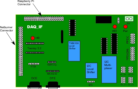
DAQ_IF
Data acquisition interface board
 High-resolution image shot with a Canon EOS 5D MII
 High-resolution image shot with a Canon EOS 5D MII
The DAQ_IF board provides the interface between a controlling single board computer (SBC) and the reset of the DAQ system. The DAQ_IF board provides the following features:
- Open Hardware design based on Creative Commons 4.0 license
- Single 5V power supply input connector (screw terminals)
- LED indicates when power is applied
- Watchdog timer actuates a relay after five-second timeout without a refresh operation (timeout period can be changed by swapping out a different resistor)
- An LED indicates current watchdog timeout state (on: watchdog okay/safe, off: watchdog trip)
- Watchdog state (relay) is available on a three-pin header (relay NO, COM, and NC contact signals)
- An LED indicates when the watchdog timer is being refreshed.
- 3.3V level shifting (from SBCs) to 5V used by the rest of the DAQ system
- Off-the-shelf support for Netburner MOD54415, Raspberry Pi, and Teensy 3.2 SBCs
- RS232 level shifting (from TTL to RS-232 levels) for one RS-232 serial port (Teensy and Raspberry Pi only)
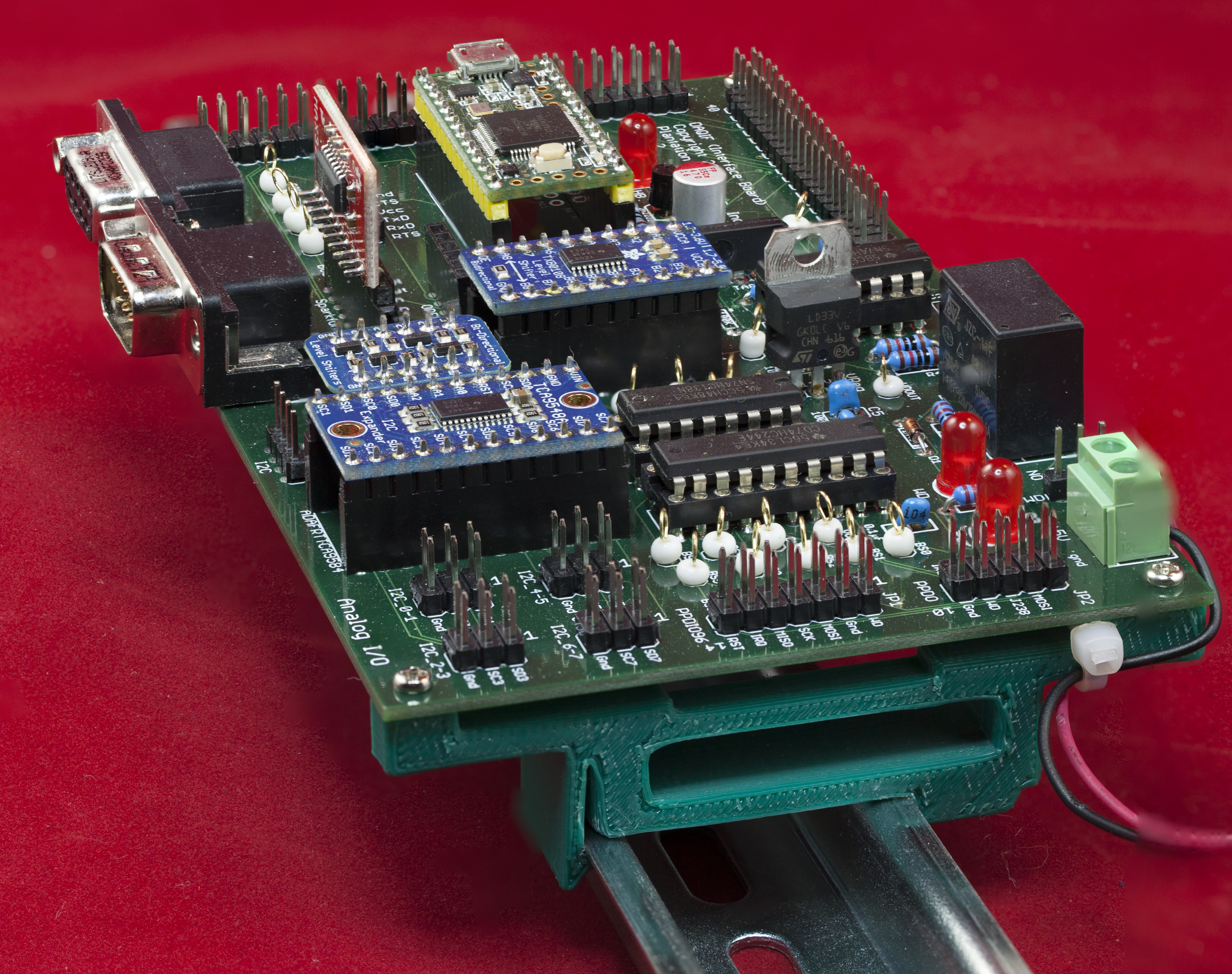
- I2C level shifting and multiplexing -- provides 8 independent I2C ports for use in the DAQ system (routed to four six-pin headers on the board)
- 4-pin I2C connector provides breakout for SBC I2C bus
- SPI bus expansion with seven independent chip select lines (routed to two headers on the board)
- Full buffering for output signals.
- Interrupt support for digital input devices
- Software-controlled reset line for resetting peripherals attached to DAQ_IF board
- User-definable I/O pin available on board
- Watchdog state is also broadcast to all peripheral boards
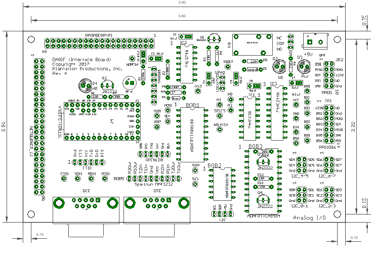
- Schematic and board layout are available in Eagle format
- DIN rail mounts allow the board to be optionally mounted in a horizontal orientation on a 35mm DIN rail
- DIN rail brackets are available in .STL format for 3D-printing
- Full documentation including System Requirements Specifications (SyRS), Hardware Requirements Specifications (HRS), Hardware Inspection list (HI), Hardware Test Cases (HTC), Hardware Test Procedures (HTP), Hardware Design Description (HDD), and (reverse) Traceability Matrix (RTM) are available for the DAQ system, including this board.
Bill of Materials (BOM) for the DAQ_IF board:
- (3) 5mm LEDs
- (1) JCZ-11F 005-1Z 5VDC relay
- (1) 74HC74 flip flop
- (1) 74HC138 3-to-8 digital decoder
- (1) 74HC244 octal buffer
- (1) TA8030S watchdog timer
- (1) Adafruit TXB0108 8-channel bi-directional level shifter
- (1) Adafruit BSS138 4-channel I2C safe bi-directional level shifter
- (1) Adafruit TCA9548A I2C Multiplexer
- (1) LD1117V33 3.3V voltage regulator
- (6) 0.1 µF decoupling capacitors
- (1) 10 µF capacitor
- (1) 47 µF capacitor
- (4) 2N2222 Transistors
- (1) 1N4733A zener diode (~4.7V)
- (1) 1N4148 diode
- (3) 220 Ω resistors (all resistors are 1%, 1/4 watt)
- (3) 390 Ω resistors
- (3) 100 kΩ resistors
- (2) 10 kΩ resistors
- (1) 1.2 kΩ resistor
- (1) 27 Ω resistor
- (1) Two-pin screw terminal (5mm/0.2" centers)
- (1) PPRelay-12 PCB
- (6) 6-pin (2x3) male headers
- (1) 4-pin (1x4) male header
- (1) 3-pin (1x3) male header
- (1) 14-pin (2x7) male header
- (1) 10-pin (2x5) male header
- (2) 14-pin (1x14) female headers
- (1) 40-pin (2x20) male header
- (1) 50-pin (2x25) male header
- Optional: (1) Sparkfun MAX3232 transceiver breakout
- Optional: (1) DB9F female DB9 RS-232 connector (right angle PCB mount)
- Optional: (1) DB9F Male DB9 RS-232 connector (right angle PCB mount)
- Optional: (1) Sparkfun Openlog RS-232 logging module
- Optional: (1) FTDI cable (USB to FTDI/RS-232 serial connection)
- Optional: (1) 6-pin (1x6) female header
- Optional: (1) 6-pin (1x6) male header
- Optional: (1) 10-pin (1x10) female header
- Optional: (27) test pins
- Optional: one set of horizontal 35mm DIN rail mounts for DAQ boards
Note: If you only want a few DAQ_IF PCBs, contact Plantation Productions (randy@plantation-productions.com) to see if there are any in stock. Bare boards are $25 each plus shipping; fully assembled and tested boards are $599. If you need more than a couple PCBs and you're not in a huge hurry, it costs about $150 (plus about 4-6 weeks) to have a set of 10 manufactured and shipped to you from China. I use Seeed Studio Fusion PCD service (https://www.seeedstudio.com/fusion.html). The PPOpto-12 PCBs are four-layer boards. Here are the Gerber files for them (provide these files to Seeed Studio or your personal PCB manufacturer).
If you want to modify or enhance the DAQ_IF design, or re-layout the PCB using Eagle, here are the Eagle files:
DAQ_IF Eagle files (Schematic and board layout)
If you simply want to view the schematic on-line, you'll find that here:
The DIN rails were created using AutoDesk's Fusion 360 (to produce STL files) and I personally print the results on a Lulzbot Taz6 3D printer using ABS filament (ABS is recommended for this job, PLA and PETG are a bit brittle). The STL files can be found here:
DAQ_IF DIN Rail Brackets 3D printer files
DAQ_IF Board Layout
DAQ_IF Compatible Single Board Computers
The DAQ_IF (DAQ system InterFace) board is a bridge between a commercially-available single-board computer (SBC) and the reset of the DAQ sysem. The DAQ_IF was designed to easily interface with any of the following SBCs:
- Netburner MOD54415 Evaluation Board (MOD54415 LC Development kit, or MOD54415 + MOD-DEV-70CR)
- Teensy 3.2
- Raspberry Pi 3 Model B (actually, any Pi with a 40-pin connector will work)
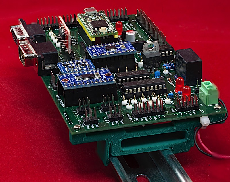
The standard firmware for the DAQ system assumes the use of the Netburner MOD54415 evaluation kit. Various DAQ test procedures use a Teensy 3.2 module (mounted directly on the DAQ_IF board; as shown in the picture above [with the yellow headers]).
In general, you can easily interface just about any SBC computer to the DAQ_IF module as long as it has the following:
- One available SPI bus and SPI chip select line (MISO, MOSI, SCK, and CS pins)
- One available I2C bus (with nothing else attached to it)
- At least 5 digital output pins (A0, A1, A2, Reset, and WD_RFSH on the DAQ_IF schematic)
- At least two input pins, one of which should be capable of generating an interrupt on the CPU (WD_LATCH_3 and IRQ on the DAQ_IF schematic)
- At least one pin that can be programmed as an input or an output pin (J2_38 on the DAQ_IF schematic)
- Optional: TTL-level RS-232 signals (Tx, Rx, RTS, and CTS; RX1, TX1, CTS1, and RTS1 on the DAQ_IF schematic).
By wiring these signals to the appropriate pins on the Raspberry Pi, Netburner, or Teensy 3.2 connectors on the DAQ_IF, you can connect almost any SBC to the DAQ system.
The DAQ_IF board assumes that the SBC uses 3.3V logic (true for the Netburner, Teensy 3.2, and Raspberry Pi). With a little rewiring (removing some level shifters and inserting jumper wires in their place) the DAQ_IF board could work with 5V/TTL-level logic; that is left as an exercise to the interested reader.
DAQ_IF Revision History
Rev 2:
Added capacitor and resistor to CLR input on 7474 (from RESET)
to prevent a constant low from keeping the WD reset.
Added 75HC244 buffers to various outputs.
Added test pin for WD_LATCH_5.
Modified reset line to TCA9548A BoB to handle +5V pullup
resistor on the BoB (Open collector xstr circuit).
Reversed Raspberry 40-pin connector.
Rev 3
Swapped P2N222 transistors for 2N2222 transistors (swaps E & C)
Changed R9 to a pullup to 3.3v, added clamp diode
Swapped RESET & WD_LATCH pins on IC3B
Rev 4:
Replaced capacitors with 3-pad variants to allow different sized
decoupling capacitors on board.
Rev 5:
Changed R2 to 10K (from 100K)
Rev 6:
Changed polarity on WD relay to make it fail safe (relay must be turned on
when NOT timed out). Had to add new transistors/resistors to invert LED.
DAQ_IF Functionality
The DAQ_IF board provides the following functionality to the DAQ system:
- Level shifting: The DAQ_IF board converts 3.3V logic levels to the 5V logic levels the rest of the DAQ system uses.
- I2C level shifting: The DAQ_IF board converts I2C signals between 3.3V and 5V.
- SPI bus expansion: The DAQ_IF board expands the single SPI chip-select line to seven separate board select lines (BS0, BS1,..., BS6).
- I2C bus expansion: The DAQ_IF board contains an Adafruit TCA9584 I2C bus multiplexor chip that expands the I2C bus to eight separate I2C busses (allowing you to attach up to eight devices with the same I2C bus to the DAQ_IF board).
- RS-232 level shifting (Teensy 3.2 and Raspberry Pi only): The DAQ_IF board includes a Sparkfun Max3232 breakout board that converts TTL-level RS-232 signals to true RS-232. DCE and DTE connections are provided on the DAQ_IF board (no need for NULL modems). Note: the Netburner MOD54415 module has its own built-in RS-232 level shifters so this circuitry can be left uninstalled on system with a Netburner SBC.
- FTDI and Openlog support (Teensy/Raspberry Pi only): In place of the MAX3232 module, you can optionally install an FTDI serial-to-USB cable or a Sparkfun Open Log module). Note: only one of the MAX3232 module, FTDI cable, or OpenLog modules may be installed on a single DAQ_IF board. Installing two or more of these devices will create conflicts that could damage the modules or the DAQ_If board.
- Five second watchdog timer with NC/COM/NO (normally closed/common/normally open) relay. Useful in safety critical systems to detect when the software has frozen. Hardware can automatically reset itself or place the system in a fail-safe mode when a watchdog timeout occurs. Timeout is nominally 5 seconds but you can easily change it by substituting a different resistor value. NO output is open on watchdog trip, closed on watchdog safe (NC is closed on watchdog trip, open on WD safe).
- Buffering for all output signals (including SPI outputs).
In addition to the above, the DAQ_IF board features LEDs indicating the following:
- Power applied
- Watchdog timeout
- Heartbeat/watchdog refresh/general purpose LED output
The DAQ_IF board also includes numerous test pins to aid in testing and maintenance of the board.
Connecting a SBC to the DAQ_IF
The DAQ_IF contains three sets of headers allowing you to connect a Netburner module, and Raspberry Pi module, or a Teensy 3.2 module.
The 50-pin male header on the left side of the DAQ_IF circuit board connects to the J2 connector on a Netburner MOD54415/MOD-DEV-70CR evaluation board. Note that you cannot connect a bare MOD54415 daughter board directly to the DAQ_IF without using the MOD-DEV-70 evaluation module. The eval module provides a power supply and several other features that the DAQ system will use. The eval module also provides DIP switches, LEDs, a USB connector, and RS-232 connectors that you may want to use. You must provide power for the Netburner module independently of the DAQ_IF board (usually through the USB connector, though you could also wire up a power supply directly to the MOD-DEV-70 board). You will need a 50-pin ribbon cable to connect the Netburner module to the DAQ_IF.
The 40-pin connector on the top/left side of the DAQ_IF board is the Raspberry Pi interface. Run a 40-pin ribbon cable from the Pi GPIO header to this connector. You must provide power for the Pi module independently of the DAQ_IF board (through the USB connector on the Pi). You will need a 40-pin ribbon cable to connect the Pi module to the DAQ_IF.
A Teensy 3.2 module mounts directly on the two 14-bit single-in-line headers on the left/center side of DAQ_IF board (the picture at the top of this page shows a Teensy 3.2 installed on the DAQ_IF board). Unlike the Netburner and Raspberry Pi modules, the Teensy 3.2 can get its power directly from the DAQ_IF board. This requires cutting the VUSB trace on the Teensy 3.2 module (see the Teensy 3.2 documentation for details). Alternately, you can feed power to the Teensy 3.2 module via the microUSB connector if you don't want to cut the VUSB trace on the Teensy board.
IMPORTANT NOTE:
You may only install one SBC on a single DAQ_IF board. If you install multiple SBCs their signals will conflict with one another and this may damage the DAQ_IF or SBCs.
Connector Other DAQ System Boards to the DAQ_IF Board
The DAQ_IF board provides six separate headers/connectors you can use to connect PPDIO96, PPRelay-12, PPSSR-16, and PPAIO-16/4 boards. There is also a four-pin I2C connector you can use to connect additional I2C devices (beyond the PPAIO-16/4 boards) and a 3-pin header connecting to the watchdog relay.
The PPDO (digital output) bus is a 10-pin connector. It has the following pinout:
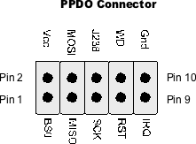
Note that the PPDO bus is an instance of the DAQ_IF SPI bus with a single chip/board select line (BS0). The PPDO bus presumes that there is a single shift register device hooked up to it (e.g., PPRelay-12 or PPSSR-16 boards). The size (in bits) of the shift register is arbitrary. In the DAQ system, each PPRelay-12 or PPSSR-16 board you daisy chain to the PPDO connector adds 16 bits to the size of the shift register. For example, if you have two PPRelay-12 and one PPSSR-16 boards daisy-chained to the PPDO connection, the shift register length is 48 bits (16 bits per board).
Note that the PPRelay-12 and PPSSR-16 boards do not use the MISO, J238, and IRQ signals. The PPRelay-12 and PPSSR-16 boards are output-only devices, so the MISO (Master input, slave output) pin has no use. Likewise, these two boards don't generate any interrupts, so these boards don't use the IRQ line. The DAQ system reserves the J238 line for end-user use, so the PPRelay-12 and PPSSR-16 boards don't use this pin.
The DAQ_IF board uses the SCK and MOSI lines to shift data into the shift registers. Although the TPIC6B595 high-current shift registers the PPRelay-12 and PPSSR-16 boards use is not, technically speaking, an SPI device, it turns out that the timing of the SPI clock (SCK) and MOSI (serial output data) signals are compatible with the serial shift clock and serial data in pins on the TPIC6B595 shift register. See the discussion of these signals on the PPRelay-12 and PPSSR-16 pages for more details.
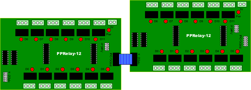
To connect one or more PPSSR-16 or PPRelay-12 boards to a DAQ_IF board, simply run a cable from the PPDO connector on the DAQ_IF board to the PPDO In connector on the first PPRelay-12 or PPSSR-16 board in the daisy chain. Connect the first and second PPRelay-12/PPSSR-16 boards together by running a cable from the PPDO Out connector on the first board to the PPDO In connector on the second. Repeat this connector for any additional PPRelay-12 or PPSSR-16 boards in the daisy chain.
By convention, the first board connected to the DAQ_IF PPDO output connector has bits DO0..DO15; the second board in the daisy chain as bits DO16..DO31; the third board has bits DO32..DO47; etc. Remember that although the PPRelay-12 has only 12 relays, it actually has 16 output bits. Four output bits do not have associated relays -- they appear on the auxiliary output connector on the PPRelay-12.
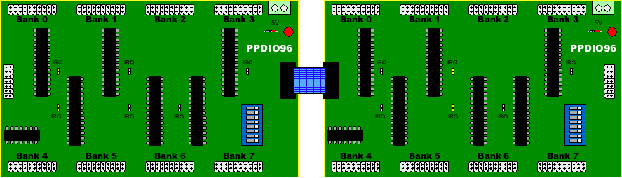
The PPDIO96 (digital I/O) bus is a 14-pin connector. It has the following pin out:
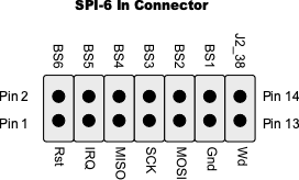
BS1..BS6 are six of the chip/board select signals from the 74HC138 decoder chip on the DAQ_IF boards. When daisy-chaining PPDIO96 boards, these board select lines allow the selection of up to six PPDIO96 boards in the daisy chain (one board select line for each board).
MISO, MOSI, and SCK are the standard SPI bus signals (the fourth signal, CS, is handled by BS1..BS6).
IRQ is an input to the DAQ_IF board from the PPDIO96 boards. When activated for a particular MCP23S17 I/O expander chip, the PPDIO96 board(s) will assert this signal (active low) when requesting interrupt service. Note that you will have to program your own interrupt service routine to process this signal, if you activate it.
The J2_38 pin is reserved for end-user use. As such, the PPDIO96 boards ignore this signal line. If you create your own circuit designs to use the PPDIO96 bus, you can use this signal for whatever purpose you desire.
The WD signal is active (low) whenever the watchdog timer has timed out. The PPDIO96 boards do not use this signal. If you create your own circuits to attach to the PPDIO96 bus, you might use this pin to force your circuitry into a fail-safe condition should a watchdog timeout occur.
Note: the PPDIO96 boards do not support fail-safe operation. If a watchdog timeout occurs, any programmed output pins will continue to output the last data written to them. The state of the MCP23S17 ICs does not change when a watchdog timeout occurs.
When the DAQ_IF board pulls the RST line line, this resets the MCP23S17 to its power-on state. This includes setting all I/O pins to inputs and disabling all internal pull-up resistors. For complete details on the MCP23S17 (power-on) reset state, please see the data sheet:
To connect one or more PPDIO96 boards to a DAQ_IF board, simply run a cable from the PPDIO96 connector on the DAQ_IF board to the PPDIO96 In connector on the first PPDIO96 board in the daisy chain. Connect the first and second PPDIO96 boards together by running a cable from the PPDIO96 Out connector on the first board to the PPDIO96 In connector on the second. Repeat this connector for any additional PPDIO96 boards in the daisy chain.
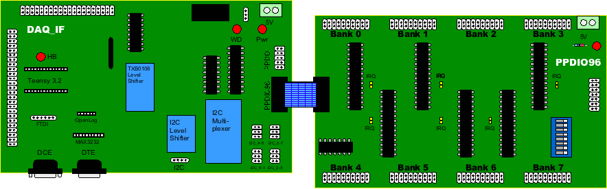
There are four six-pin I2C headers on the DAQ_IF board. Each header contains two independent I2C busses. These I2C busses connect to the PPAIO-16/4 boards and you can daisy-chain up to two PPAIO-16/4 boards on each I2C connector.
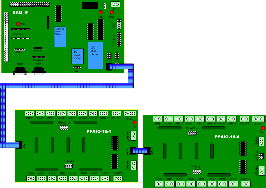
By connecting two PPAIO-16/4 boards to each I2C connection, you can connect a total of 8 PPAIO-16/4 boards to a single DAQ_IF board.
By convention you should attach the first four boards to the four I2C connectors on the DAQ_IF board before daisy-chaining any PPAIO-16/4 boards. The standard firmware makes the following associations on the I2C busses:
| I2C port | AINx Range First board :: Daisy-chaned board |
AOUTx Range First board :: Daisy-chaned board |
|---|---|---|
| I2C_0-1 | AIN0-AIN15 :: AIN64-AIN79 | AOUT0-AOUT3 :: AOUT16-AOUT19 |
| I2C_2-3 | AIN16-AIN31 :: AIN80-AIN95 | AOUT4-AOUT7 :: AOUT20-AOUT23 |
| I2C_4-5 | AIN32-AIN47 :: AIN96-AIN111 | AOUT8-AOUT11 :: AOUT24-AOUT27 |
| I2C_6-7 | AIN48-AIN63 :: AIN112-AIN127 | AOUT11-AOUT15 :: AOUT28-AOUT31 |
Programming the DAQ_IF Board
Obviously, the specifics of programming the DAQ_IF board depends on what SBC you are using and which other modules in the DAQ system you've attached to the DAQ_IF. However, there are a few things you should be aware of when writing your own code for the DAQ_IF board.
I2C Bus Multiplexor
The Adafruit TCA9548A Breakout Board (BoB) responds to I2C address 0x70. Writing a byte to this I2C address with a single bit set will activate the corresponding I2C bus on the DAQ_IF board (there are 8 I2C busses -- I2C_0 through I2C_7). Writing a one in bit position zero makes bus I2C_0 active; writing a one to bit position 1 makes bus I2C_1 active; etc. Once a bus is active, it remains active until you write a different value to the TCA9548A BoB. Writing a zero to the TCA9548A BoB disables all eight I2C busses on the multiplexor.
Note: how you write a byte to I2C address 0x70 is SBC-dependent and beyond the scope of this discussion. See the sample code for the different SBCs to see how to do this for the Teensy 3.2, Raspberry Pi, and Netburner SBCs.
Reset
Programming a low pulse on the reset output pin will send a reset signal to all the devices in the DAQ system. You must program this pin low for at least 250 msec. The reset signal has the following effects throughout the system:
- Resets the watchdog timer. Note that this is the only way to reset the watchdog timer latch. Therefore, you should always send a reset pulse when the system first powers up.
- Resets the MCP23S17 GPIO expander chips on the PPDIO96 boards attached to the DAQ_IF. Note that this reprograms all the digital I/O pins as inputs and disables all pull-up resistors. If you've programming any pins as outputs or if you've enabled any programmable pull-up resistors on the MCP23S18, you will need to reinitialize the I/O expander after pulsing the reset line.
- Puts all the output relays on the PPRelay-12 and PPSSR-16 boards in fail-safe mode (open relay contacts).
Watchdog Refresh
Programming a rising edge on the WD_RFSH output pin will refresh the DAQ_IF's on-board watchdog timer hardware. You must program at least one pulse every five seconds (or faster) to prevent the watchdog timer from "timing out" and activating the watchdog timer relay.
The WD_RFSH line also drives the HB (heartbeat) LED on the DAQ_IF board. If you arrange your watchdog refresh code so that it inverts the WD_RFSH line every 1/2 second, this will creating a blinking HB LED that indicates that the system is running. If the HB LED freezes (either on or off), this indicates a problem with the software (above and beyond the watchdog timeout that will occur five seconds after the timer is no longer refreshed).
Watchdog Latch Input
The watchdog latch input pin gives you an indication of the current watchdog timeout state. If you read a '1' on this input pin, then the watchdog timer has latched the "timeout" state. If you read a '0' on this pin, the watchdog timer has not timed out.
Note that once the watchdog timer times out, the watchdog timeout state is latched until the software explicitly resets it. Note that refreshing the watchdog timer once it has timed out will not reset the watchdog timer. You must pulse the reset signal (as noted above) to reset the watchdog timer.
IRQ Input
The IRQ input signal is connected to the INTA lines on the MCP23S17 I/O expanders found on the PPDIO96 board. Note that the IRQ jumper with a given MCP23S17 must be installed for this signal to work. If you want to use this feature on the DAQ_IF you'd normally program the associated input pin on the SBC as an interrupt and write an interrupt service routine to process the interrupt. You could also poll this input pin if writing an interrupt service routine isn't appropriate.
J2_38 Pin
The J2_38 pin is an application-defined I/O pin. The DAQ system firmware does not use this pin; it's left for your own use.
BTW: this pin gets its name from the Netburner board. It's pin 38 on header J2.
SPI Bus Programming
The DAQ_IF provides a 74HC138 3-to-8 decoder to provide SPI bus chip select expansion. The 74HC138 has four input pins: the SPI chip select pin (which acts as a chip select to the 74HC138 IC) and three SPI address lines: pins A0, A1, and A2. To program a specific SPI device you must first program output pins A0, A1, and A2 with a three-bit binary number. Then you activate the SPI chip select line and do the SPI transmission. When the transmission is complete, you deactivate the SPI chip select line (note: activating and deactivating the SPI chip select line is often handled in library code or by hardware -- you might not need to explicitly program this pin).
The DAQ system reserves the eight possible chip select lines (BS0, BS1, ..., BS7) for the following purposes:
- BS0 (used by/shared byPPRelay-12 and PPSSR-16 boards)
- BS1: selects the first PPDIO96 board in the daisy chain.
- BS2: selects the second PPDIO96 board in the daisy chain.
- BS3: selects the third PPDIO96 board in the daisy chain.
- BS4: selects the fourth PPDIO96 board in the daisy chain.
- BS5: selects the fifth PPDIO96 board in the daisy chain.
- BS6: selects the sixth PPDIO96 board in the daisy chain.
- BS7 is reserved to mean "no board selected".
Note that you could design your own SPI-bus device and connect it to the PPDIO96 bus on the DAQ_IF board; however, keep in mind that the standard firmware assumes you've got PPRelay-12 and PPSSR-16 boards on BS0 and PPDIO96 boards on BS1..BS6.
PPDO Programming
As mentioned earlier, the boards daisy-chained to the PPDO connector look like a single shift register to the DAQ_IF board. Adding more PPRelay-12 or PPSSR-16 boards to the daisy chain (specifications allow a maximum of 10 boards -- this is limited by TTL fanout) extends the size of the shift register by 16 bits for each board you add.
To program this "shift register" you must first pull the BS0 line low. Next, you transmit the specified number of bytes (two bytes for each board in the daisy chain) via the SPI libraries. Finally, you set the BS0 line high. On the rising edge of the BS0 signal line, the TPIC6B595 shift registers transfer the data from the internal shift registers to the output latches. Note that during the shift operation, the data on the TPIC6B595 output pins (controlling the relays) does not change until the rising edge of the BS0 signal.
Because of the nature of shift registers, if you shift extra data to the shift registers (more than n*2 bytes, where n is the number of daisy-chained boards) then the extra data is lost (the extra data will be the first bytes you shift out). Because of the wiring of the daisy-chain, the last two data bytes you shift out will be shifted into the first board in the daisy chain (the board connected directly to the DAQ_IF board), the two bytes shifted out before the last two bytes will be shifted into the second board of the daisy chain, etc.
Toggling the DAQ_IF reset line will immediately clear all the TPIC6B595 shift registers and output latches. While the reset line is low, the PPRelay-12 and PPSSR-16 boards will force the internal shift registers to all zero bits. On the rising edge of the reset line, the boards will transfer the data (now zeros) from the internal shift registers to the output latches. Note that if you are in the middle of shifting data into the shift registers while also pulsing the reset line (say, in a multi-threaded environment), the results are undefined. If you must shift data into the shift register from one thread and you could be toggling the reset line from a separate thread, you should use synchronization primitives to protect access to the SPI clock.
If the watchdog timer times out and asserts the WD signal on the PPDO connector, the PPRelay-12 and PPSSR-16 boards will automatically put the output relays in a fail-safe mode by clearing the internal shift register and transferring their contents to the TPIC6B595 output latches. As for the reset line, if you're currenting shifting data into the shift register when the WD timer times out, this could create an undefined result. In theory, the software has hung up and probably isn't shifting data to the PPDO connector. In practice, this could be the result of some operation taking too long. To prevent this undefined operation, it's a good idea to always refresh the watchdog timer immediately prior to shifting out any data and checking the WD_LATCH value to ensure that the watchdog timer hasn't already timed out.
For information about the TPIC6B595 serial in/parallel out high-current shift register, please consult the data sheet.
TPIC6B595 shift register data sheet
PPDIO96 Programming
Each PPDIO96 board contains six MCP23S17 GPIO expansion ICs. These are very flexible 16-bit general-purpose I/O expanders. To program a particular MCP23S17 you must set the appropriate board select pin (BS1..BS6) low by programming the A0, A1, and A2 output pins on the DAQ with the binary number (1..6) of the board you wish to select. You address the six MCP23S17 ICs on a PPDIO96 board by using the IC number (2..7) on the board as the address for that particular chip. Beyond that, it's just standard MCP23S17 programming (see the data sheet).
For more details on programming PPDIO96 boards, see the PPDIO96 web page.
Although the PPDIO96 bus/connector was specifically intended for use with DAQ system PPDIO96 boards, this connector is really nothing more than an expanded SPI bus connector. You can easily attach other SPI devices to this bus and program them just as you would any other SPI device. That programming activity is left to the interested reader; obviously it's beyond the scope of this documentation.
I2C Programming
The DAQ_IF board contains an I2C connection and an Adafruit TCA9548A I2C multiplexor/breakout board with 8 independent I2C busses distributed across four six-pin headers. All I2C busses are controlled by a single I2C bus coming from the SBC (Netburner, Raspberry Pi, or Teensy 3.2). The TCA9548A I2C multiplexor responds to I2C address 0x70. Writing a zero byte to this I2C address disables the eight busses coming out of the multiplexer. Writing a bit with a single '1' bit activates the bus corresponding to the bit position of the '1':
| Byte Written to 0x70 | Bus Enabled |
|---|---|
0 |
None (main I2C bus on 4-pin header is still active) |
1 |
I2C_0 |
2 |
I2C_1 |
4 |
I2C_2 |
8 |
I2C_3 |
16 (0x10) |
I2C_4 |
32 (0x20) |
I2C_5 |
64 (0x40) |
I2C_6 |
128 (0x80) |
I2C_7 |
The PPAIO-16/4 boards utilize Adafruit ADS1116 16-bit ADC breakout boards that respond to I2C addresses 0x48..0x4b. These boards also utilize Adafruit and Sparkfun MCP4725 12-bit DAC breakout boards that respond to I2C addresses 0x60..0x63. If you attach any I2C devices to the 4-pin I2C header on the DAQ_IF board (or any of the 6-pin I2C headers controlled by the TCA9548A) you should make sure your device(s) don't use these same addresses (or 0x70, used by the TCA9548A).
Programming the ADS1115 ADC or MCP4725 DAC is most easily accomplished using the library code provided by Adafruit and Sparkfun (it may need to be ported from Arduino form to Netburner or Raspberry Pi form). Of course, you can always use the library code provided with the DAQ system standard firmware.