
1.4 System Timing
Although modern computers are quite fast and getting faster all the time, they still require a finite amount of time to accomplish even the smallest tasks. On Von Neumann machines like the 80x86, most operations are serialized. This means that the computer executes commands in a prescribed order. It wouldn't do, for example, to execute the statement I:=I*5+2; before I:=J; in the following sequence:
		I := J;

		I := I * 5 + 2;
Clearly we need some way to control which statement executes first and which executes second.
Of course, on real computer systems, operations do not occur instantaneously. Moving a copy of J into I takes a certain amount of time. Likewise, multiplying I by five and then adding two and storing the result back into I takes time. As you might expect, the second Pascal statement above takes quite a bit longer to execute than the first. For those interested in writing fast software, a natural question to ask is, "How does the processor execute statements, and how do we measure how long they take to execute?"
The CPU is a very complex piece of circuitry. Without going into too many details, let us just say that operations inside the CPU must be very carefully coordinated or the CPU will produce erroneous results. To ensure that all operations occur at just the right moment, the 80x86 CPUs use an alternating signal called the system clock.
1.4.1 The System Clock
At the most basic level, the system clock handles all synchronization within a computer system. The system clock is an electrical signal on the control bus which alternates between zero and one at a periodic rate (see Figure 1.10). All activity within the CPU is synchronized with the edges (rising or falling) of this clock signal.
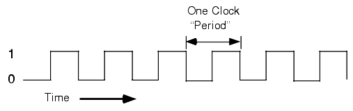
The frequency with which the system clock alternates between zero and one is the system clock frequency. The time it takes for the system clock to switch from zero to one and back to zero is the clock period. One full period is also called a clock cycle. On most modern systems, the system clock switches between zero and one at rates exceeding several hundred million times per second to several billion times per second. The clock frequency is simply the number of clock cycles which occur each second. A typical Pentium IV chip, circa 2002, runs at speeds of 2 billion cycles per second or faster. "Hertz" (Hz) is the technical term meaning one cycle per second. Therefore, the aforementioned Pentium chip runs at 2000 million hertz, or 2000 megahertz (MHz), also known as two gigahertz. Typical frequencies for 80x86 parts range from 5 MHz up to several Gigahertz (GHz, or billions of cycles per second) and beyond. Note that one clock period (the amount of time for one complete clock cycle) is the reciprocal of the clock frequency. For example, a 1 MHz clock would have a clock period of one microsecond (1/1,000,000th of a second). Likewise, a 10 MHz clock would have a clock period of 100 nanoseconds (100 billionths of a second). A CPU running at 1 GHz would have a clock period of one nanosecond. Note that we usually express clock periods in millionths or billionths of a second.
To ensure synchronization, most CPUs start an operation on either the falling edge (when the clock goes from one to zero) or the rising edge (when the clock goes from zero to one). The system clock spends most of its time at either zero or one and very little time switching between the two. Therefore clock edge is the perfect synchronization point.
Since all CPU operations are synchronized around the clock, the CPU cannot perform tasks any faster than the clock. However, just because a CPU is running at some clock frequency doesn't mean that it is executing that many operations each second. Many operations take multiple clock cycles to complete so the CPU often performs operations at a significantly lower rate.
1.4.2 Memory Access and the System Clock
Memory access is one of the most common CPU activities. Memory access is definitely an operation synchronized around the system clock or some submultiple of the system clock. That is, reading a value from memory or writing a value to memory occurs no more often than once every clock cycle. Indeed, on many 80x86 processors, it takes several clock cycles to access a memory location. The memory access time is the number of clock cycles the system requires to access a memory location; this is an important value since longer memory access times result in lower performance..
Memory access time is the amount of time between a memory operation request (read or write) and the time the memory operation completes. Modern x86 CPUs are so much faster than memory that systems built around these CPUs often use a second clock, the bus clock, that is some sub-multiple of the CPU speed. For example, typical processors in the 100 MHz to 2 GHz range use 400MHz, 133MHz, 100MHz, or 66 MHz bus clocks (often, the bus speed is selectable on the CPU).
When reading from memory, the memory access time is the amount of time from the point that the CPU places an address on the address bus and the CPU takes the data off the data bus. On typical x86 CPU with a one cycle memory access time, a read looks something like shown in Figure 1.11.Writing data to memory is similar (see Figure 1.12).
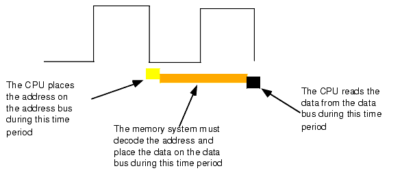
Figure 1.11 The 80x86 Memory Read Cycle
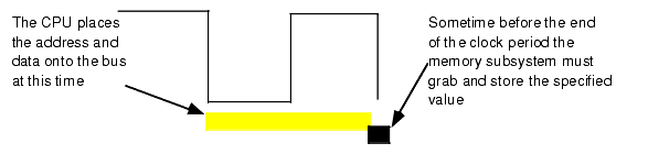
Figure 1.12 The 80x86 Memory Write Cycle
Note that the CPU doesn't wait for memory. The access time is specified by the bus clock frequency. If the memory subsystem doesn't work fast enough, the CPU will read garbage data on a memory read operation and will not properly store the data on a memory write operation. This will surely cause the system to fail.
Memory devices have various ratings, but the two major ones are capacity and speed (access time). Typical dynamic RAM (random access memory) devices have capacities of 512 (or more) megabytes and speeds of 0.25-100 ns. You can buy bigger or faster devices, but they are much more expensive. A typical 2 GHz Pentium system uses 2.5 ns (400 MHz) memory devices.
Wait just a second here! At 2 GHz the clock period is roughly 0.5 ns. How can a system designer get away with using 2.5 ns memory? The answer is wait states.
1.4.3 Wait States
A wait state is nothing more than an extra clock cycle to give some device time to complete an operation. For example, a 100 MHz Penitum system has a 10 ns clock period. This implies that you need 10 ns memory. In fact, the situation is worse than this. In most computer systems there is additional circuitry between the CPU and memory: decoding and buffering logic. This additional circuitry introduces additional delays into the system (see Figure 1.13). In this diagram, the system loses 10ns to buffering and decoding. So if the CPU needs the data back in 10 ns, the memory must respond in less than 0 ns (which is impossible).
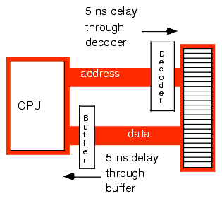
Figure 1.13 Decoding and Buffer Delays
If cost-effective memory won't work with a fast processor, how do companies manage to sell fast PCs? One part of the answer is the wait state. For example, if you have a 2 GHz processor with a memory cycle time of 0.5 ns and you lose 2 ns to buffering and decoding, you'll need 2.5 ns memory. What if your system can only support 10 ns memory (i.e., a 100 MHz system bus)? Adding three wait states to extend the memory cycle to 10 ns (one bus clock cycle) will solve this problem.
Almost every general purpose CPU in existence provides a signal on the control bus to allow the insertion of wait states. Generally, the decoding circuitry asserts this line to delay one additional clock period, if necessary. This gives the memory sufficient access time, and the system works properly (see Figure 1.14).
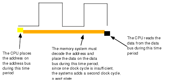
Figure 1.14 Inserting a Wait State into a Memory Read Operation
Needless to say, from the system performance point of view, wait states are not a good thing. While the CPU is waiting for data from memory it cannot operate on that data. Adding a single wait state to a memory cycle on a typical CPU doubles the amount of time required to access the data. This, in turn, halves the speed of the memory access. Running with a wait state on every memory access is almost like cutting the processor clock frequency in half. You're going to get a lot less work done in the same amount of time.
However, we're not doomed to slow execution because of added wait states. There are several tricks hardware designers can play to achieve zero wait states most of the time. The most common of these is the use of cache (pronounced "cash") memory.
1.4.4 Cache Memory
If you look at a typical program (as many researchers have), you'll discover that it tends to access the same memory locations repeatedly. Furthermore, you also discover that a program often accesses adjacent memory locations. The technical names given to this phenomenon are temporal locality of reference and spatial locality of reference. When exhibiting spatial locality, a program accesses neighboring memory locations. When displaying temporal locality of reference a program repeatedly accesses the same memory location during a short time period. Both forms of locality occur in the following Pascal code segment:
		for i := 0 to 10 do

			A [i] := 0;
There are two occurrences each of spatial and temporal locality of reference within this loop. Let's consider the obvious ones first.
In the Pascal code above, the program references the variable i several times. The for loop compares i against 10 to see if the loop is complete. It also increments i by one at the bottom of the loop. The assignment statement also uses i as an array index. This shows temporal locality of reference in action since the CPU accesses i at three points in a short time period.
This program also exhibits spatial locality of reference. The loop itself zeros out the elements of array A by writing a zero to the first location in A, then to the second location in A, and so on. Assuming that Pascal stores the elements of A into consecutive memory locations, each loop iteration accesses adjacent memory locations.
There is an additional example of temporal and spatial locality of reference in the Pascal example above, although it is not so obvious. Computer instructions that tell the system to do the specified task also reside in memory. These instructions appear sequentially in memory - the spatial locality part. The computer also executes these instructions repeatedly, once for each loop iteration - the temporal locality part.
If you look at the execution profile of a typical program, you'd discover that the program typically executes less than half the statements. Generally, a typical program might only use 10-20% of the memory allotted to it. At any one given time, a one megabyte program might only access four to eight kilobytes of data and code. So if you paid an outrageous sum of money for expensive zero wait state RAM, you wouldn't be using most of it at any one given time! Wouldn't it be nice if you could buy a small amount of fast RAM and dynamically reassign its address(es) as the program executes?
This is exactly what cache memory does for you. Cache memory sits between the CPU and main memory. It is a small amount of very fast (zero wait state) memory. Unlike normal memory, the bytes appearing within a cache do not have fixed addresses. Instead, cache memory can reassign the address of a data object. This allows the system to keep recently accessed values in the cache. Addresses that the CPU has never accessed or hasn't accessed in some time remain in main (slow) memory. Since most memory accesses are to recently accessed variables (or to locations near a recently accessed location), the data generally appears in cache memory.
Cache memory is not perfect. Although a program may spend considerable time executing code in one place, eventually it will call a procedure or wander off to some section of code outside cache memory. In such an event the CPU has to go to main memory to fetch the data. Since main memory is slow, this will require the insertion of wait states.
A cache hit occurs whenever the CPU accesses memory and finds the data in the cache. In such a case the CPU can usually access data with zero wait states. A cache miss occurs if the CPU accesses memory and the data is not present in cache. Then the CPU has to read the data from main memory, incurring a performance loss. To take advantage of locality of reference, the CPU copies data into the cache whenever it accesses an address not present in the cache. Since it is likely the system will access that same location shortly, the system will save wait states by having that data in the cache.
As described above, cache memory handles the temporal aspects of memory access, but not the spatial aspects. Caching memory locations when you access them won't speed up the program if you constantly access consecutive locations (spatial locality of reference). To solve this problem, most caching systems read several consecutive bytes from memory when a cache miss occurs1. 80x86 CPUs, for example, read beween 16 and 64 bytes at a shot (depending upon the CPU) upon a cache miss. If you read 16 bytes, why read them in blocks rather than as you need them? As it turns out, most memory chips available today have special modes which let you quickly access several consecutive memory locations on the chip. The cache exploits this capability to reduce the average number of wait states needed to access memory.
If you write a program that randomly accesses memory, using a cache might actually slow you down. Reading 16 bytes on each cache miss is expensive if you only access a few bytes in the corresponding cache line. Nonetheless, cache memory systems work quite well in the average case.
It should come as no surprise that the ratio of cache hits to misses increases with the size (in bytes) of the cache memory subsystem. The 80486 chip, for example, has 8,192 bytes of on-chip cache. Intel claims to get an 80-95% hit rate with this cache (meaning 80-95% of the time the CPU finds the data in the cache). This sounds very impressive. However, if you play around with the numbers a little bit, you'll discover it's not all that impressive. Suppose we pick the 80% figure. Then one out of every five memory accesses, on the average, will not be in the cache. If you have a 50 MHz processor and a 90 ns memory access time, four out of five memory accesses require only one clock cycle (since they are in the cache) and the fifth will require about 10 wait states2. Altogether, the system will require 15 clock cycles to access five memory locations, or three clock cycles per access, on the average. That's equivalent to two wait states added to every memory access. Doesn't sound as impressive, does it?
There are a couple of ways to improve the situation. First, you can add more cache memory. This improves the cache hit ratio, reducing the number of wait states. For example, increasing the hit ratio from 80% to 90% lets you access 10 memory locations in 20 cycles. This reduces the average number of wait states per memory access to one wait state in our 80486 example - a substantial improvement. Alas, you can't pull an 80486 chip apart and solder more cache onto the chip. However, modern Pentium CPUs have a significantly larger cache than the 80486 and operates with fewer average wait states.
Another way to improve performance is to build a two-level caching system. Many 80486 systems work in this fashion. The first level is the on-chip 8,192 byte cache. The next level, between the on-chip cache and main memory, is a secondary cache built on the computer system circuit board (see Figure 1.15). Pentiums and later chips typically move the secondary cache onto the same chip carrier as the CPU (that is, Intel's designers have included the secondary cache as part of the CPU module).
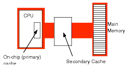
Figure 1.15 A Two Level Caching System
A typical secondary cache contains anywhere from 32,768 bytes to one megabyte of memory. Common sizes on PC subsystems are 256K, 512K, and 1024 Kbytes (1 MB) of cache.
You might ask, "Why bother with a two-level cache? Why not use a 262,144 byte cache to begin with?" Well, the secondary cache generally does not operate at zero wait states. The circuitry to support 262,144 bytes fast memory would be very expensive. So most system designers use slower memory which requires one or two wait states. This is still much faster than main memory. Combined with the on-chip cache, you can get better performance from the system.
Consider the previous example with an 80% hit ratio. If the secondary cache requires two cycles for each memory access and three cycles for the first access, then a cache miss on the on-chip cache will require a total of six clock cycles. All told, the average system performance will be two clocks per memory access. Quite a bit faster than the three required by the system without the secondary cache. Furthermore, the secondary cache can update its values in parallel with the CPU. So the number of cache misses (which affect CPU performance) goes way down.
You're probably thinking, "So far this all sounds interesting, but what does it have to do with programming?" Quite a bit, actually. By writing your program carefully to take advantage of the way the cache memory system works, you can improve your program's performance. By co-locating variables you commonly use together in the same cache line, you can force the cache system to load these variables as a group, saving extra wait states on each access.
If you organize your program so that it tends to execute the same sequence of instructions repeatedly, it will have a high degree of temporal locality of reference and will, therefore, execute faster.
1.5 Putting It All Together
This chapter has provided a quick overview of the components that make up a typical computer system. The remaining chapters in this volume will expand upon these comments to give you a complete overview of computer system organization.
1Engineers call this block of data a cache line.
2Ten wait states were computed as follows: five clock cycles to read the first four bytes (10+20+20+20+20=90). However, the cache always reads 16 consecutive bytes. Most memory subsystems let you read consecutive addresses in about 40 ns after accessing the first location. Therefore, the 80486 will require an additional six clock cycles to read the remaining three double words. The total is 11 clock cycles or 10 wait states.
|