
Note: All photographs appearing on this page are freely usable for any purpose. Links to high-resolution versions of the pictures appear below each picture.
Digital Data Acquisition & Control System
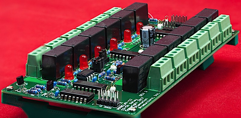
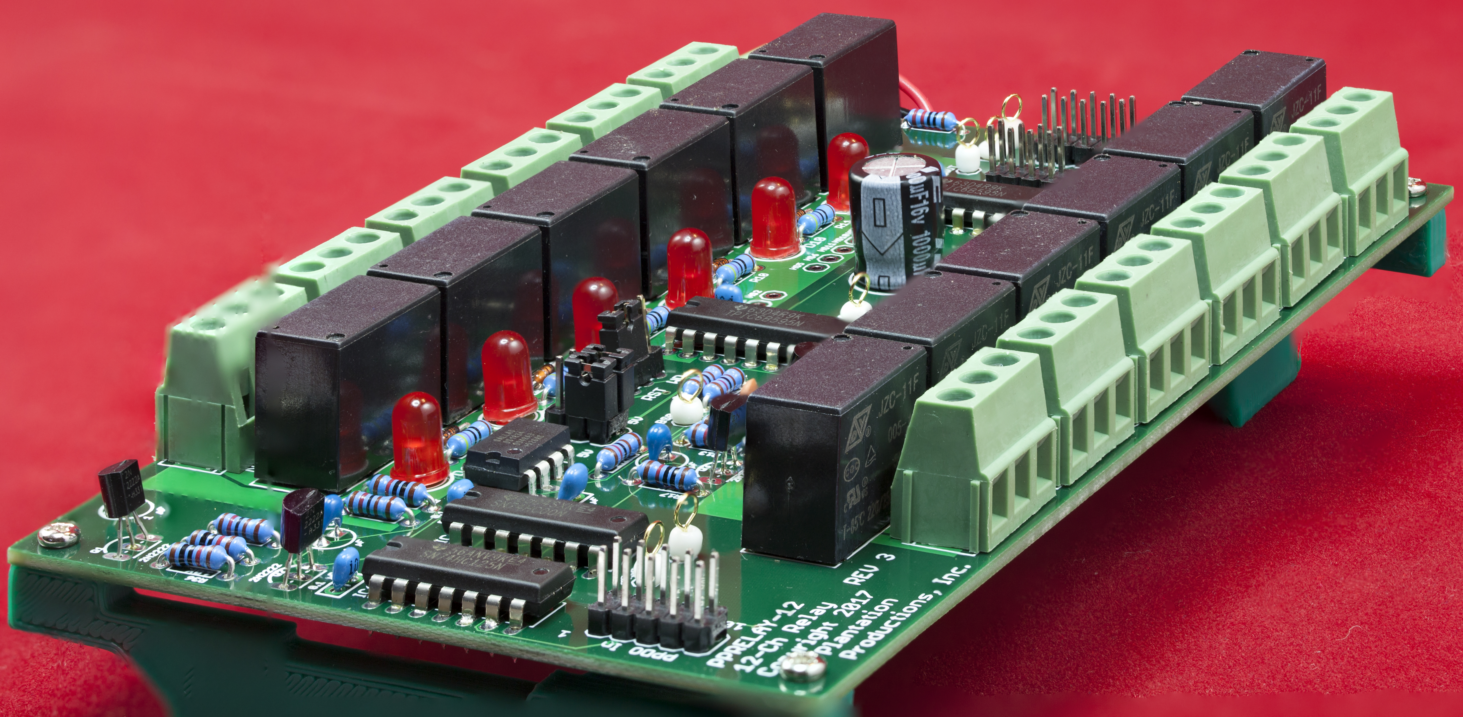
PPRelay-12
12-Channel mechanical relay/digital output board + 4-channel digital output
High-resolution image shot with a Canon EOS 5D MII
The PPRelay-12 board is a 12-channel digital output board featuring mechanical relays for 12 of the outputs. It normally connects to the DAQ_IF board via the PPDO bus. The PPRelay-12 has the following features:
- Open Hardware design based on Creative Commons 4.0 license
- Single 5V power supply input connector (screw terminals)
- LED indicates when power is applied
- 12 independent digital output channels featuring high-amperage relays (rated at 5 amps each, though the board allows 2A per relay)
- 12 LEDs indicate the current state of each output channel
- 12 three-pin screw terminal output connectors with NO (normally open), COM (common), and NC (normally closed) contacts
- Each channel is completely isolated from the output control circuit
- Four additional digital outputs are available on the aux output connector; each pin is capable of sinking up to 150 mA
- (2) PPDO-compatible ribbon cable connectors (10-pin) -- one for input and one for output (to support daisy-chaning)
- Schematic and board layout are available in Eagle format
- DIN rail mounts allow the board to be optionally mounted in a horizontal orientation on a 35mm DIN rail
- DIN rail brackets are available in .STL format for 3D-printing
- Full documentation including System Requirements Specifications (SyRS), Hardware Requirements Specifications (HRS), Hardware Inspection list (HI), Hardware Test Cases (HTC), Hardware Test Procedures (HTP), Hardware Design Description (HDD), and (reverse) Traceability Matrix (RTM) are available for the DAQ system, including this board.
Bill of Materials (BOM) for the PPRelay-12 board:
- (13) 5mm LEDs
- (12) JCZ-11F 005-1Z 5VDC relays
- (12) 1N4148 diodes
- (12) 470 Ω resistors
- (5) 0.1 µF decoupling capacitors
- (1) 1000 µF electrolytic capacitor
- (1) 74HC125 quad tri-state buffer
- (2) TPIC6B595 8-bit serial-in/parallel out high-current shift registers
- (12) 3-pin screw terminals (5mm/0.2" centers)
- (1) 2-pin screw terminal (5mm/0.2" centers)
- (1) 8-pin (2x4) male header
- (2) 10-pin (2x5) male headers
- (1) PPRelay-12 PCB
- Optional: (19) test pins
- Optional: one set of horizontal 35mm DIN rail mounts for DAQ boards
Note: If you only want a few PPRelay-12 PCBs, contact Plantation Productions (randy@plantation-productions.com) to see if there are any in stock. Bare boards are $25 each plus shipping; fully assembled and tested boards are $350 each. If you need more than a couple PCBs and you're not in a huge hurry, it costs about $150 (plus about 4-6 weeks) to have a set of 10 manufactured and shipped to you from China. I use Seeed Studio Fusion PCD service (https://www.seeedstudio.com/fusion.html). The PPRelay-12 PCBs are four-layer boards. Here are the Gerber files for them (provide these files to Seeed Studio or your personal PCB manufacturer).
PPRelay-12 Gerber Files for PCB
If you want to modify or enhance the PPRelay-12 design, or re-layout the PCB using Eagle, here are the Eagle files:
PPRelay-12 Eagle files (Schematic and board layout)
If you simply want to view the schematic on-line, you'll find that here:
The DIN rails were created using AutoDesk's Fusion 360 (to produce STL files) and I personally print the results on a Lulzbot Taz6 3D printer using ABS filament (ABS is recommended for this job, PLA and PETG are a bit brittle). The STL files can be found here:
PPRelay-12 DIN Rail Brackets 3D printer files
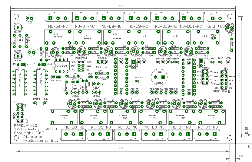
PPRelay-12 Board Layout
Connecting a PPRelay-12 board to a DAQ system
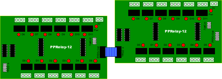
Up to 10 PPRelay-12 and/or PPSSR-16 (solid-state relay) boards can be daisy-chained together and connected to a single DAQ_IF board. You connect the first board in the daisy-chain directly to the PPDO connection on the DAQ_IF board:
You daisy-chain additional boards (PPRelay-12 or PPSSR-16) by connecting the PPDO Out connector on one board to the PPDO In connector on the next board:
The PPRelay-12 presents one TTL load to all the SPI bus signals. The DAQ_IF board buffers all SPI output signals put on the PPDO bus. Therefore, you can realistically expect a limit of about 10 daisy-chained boards on the PPDO bus. In theory, you could put as many boards in the daisy-chain as you like; however, TTL fanout and trace/ribbon cable length limit you to about 10 boards.
Because the PPDO connector carries high-frequency SPI bus signals, you should try to keep the connecting ribbon cables as short as possible. Excessively long cables may reduce the maximum number of boards you can add to the daisy chain.
Relay Connections
The contacts on each of the 12 relays on the PPRelay-12 board are routed to a 3-pin screw terminal block. These pins are the Normally Open (NO), Common (COM), and Normally Closed (NC) contacts. The relays themselves (JCZ-11F 005-1Z 5VDC) are rated for 5A operation. In practice, of course, you do not operate an electronic device at its absolute maximum rated value. Good engineering practice suggests that you derate a device by 50%. Therefore 2.5A is a more reasonable choice the maximum current you should put through one of these relays. The PPRelay-12 board has 100 mil traces (top and bottom layers) from the relay contacts to the associated screw terminal pins. Therefore, it is probably safe to run these guys with as much as 2.0-2.5 amps without worrying about the PCB heating up too much.
By their design, mechanical relays offer a fair amount of isolation beween the relay contacts and the rest of the circuit. However, PPRelay-12 boards are rated for 30VDC at the relay contacts. While the relays themselves are rated for 125VAC, putting such voltages directly on the PPRelay-12 board is unsafe. Furthermore, if any high voltage transients occur on the relay contacts, you may get arcing between traces on the PCB. If you need to handle higher voltages, use the relay contacts to actuate a separate relay (far away from the PPRelay-12 board) to switch the actual voltage.
AUXOUT Connector
The two TPIC6B595 shift register provide 16 output bits on the PPRelay-12 board. However, there are only 12 relays onboard (this is because only 12 three-pin screw terminals would fit on the standard-DAQ-system-sized PCB). The remaining four bits are brought out to an 8-pin (2x4) AUXOUT header with the following pinout:
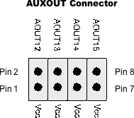
Note that the "output" pins on the TPIC6B595 IC are actually open drain outputs. Therefore the shift register sinks current, it does not source current. For this reason the alternate pin on the AUXOUT header connect to +5V (Vcc) rather than ground. From the point of view of whatever connects to these pins, the AOUT12..AOUT15 pins are the ground. Each pin on the TPIC6B595 can sink as much as 150 mA. For more details, consult the TPIC6B595 data sheet:
DS1834Sel Jumper
The DS1834SEL jump is a 6-pin header on the board:
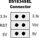
There are always two jumpers installed on this header. One jumper (between the Vcc pin and either the 3.3v or 5V pins on the right side of the header) direct the PPRelay-12's Vcc line (which is +5V) to either the 3.3v or 5V size of the DS1834 power-on reset chip. The other jumper routes the DS1834 3.3V reset or 5V reset pin to the PPRelay-12 reset circuitry. The two jumpers are not independent - both jumpers must be set to 3.3V or both jumpers must be set to 5V.
If you're wondering why you would want to route Vcc (5V) to the DS1834, well, it has to do with power-supply tolerance. The DS1834 is programmed with a 10% tolerance. If the power supply drops more than 10% below the rated voltage (typically 5V in the DAQ system) then it forces a reset output. Unfortunately, every time you turn on a relay you get a slight voltage drop on the power supply. By the time you turn on all 12 relays, it might be possible for the voltage to have dropped to just about 10%; this can be particularly problematic if your 5V power supply is low to begin with or you use higher-gauge wires as your power supply.
The PPRelay-12 board uses the DS1834 as a power-on reset, not as a brown-out protection. Therefore, if you start having problems with the relays all reseting once they're all powered on, consider switching the DS1834SEL jumpers from 5V to 3.3V. This allows the voltage to drop down to 3V before the system will reset the relays. Note that applying 5V to the DS1834 3.3V sense input will not damage the IC - all inputs (including the 3.3V sense input) are rated for 5V. For more information about the DS1834 power on reset chip, please consult the data sheet:
DS1834 Power On Reset Data Sheet (PDF)
SRCLR Selection Jumper
The SRCLR jumper is a 3-pin header on the board:
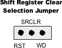
There will always be a jumper present on this header; the jump will either connect the RST and SRCLR pins or it will connect the WD and SRCLR pins.
This pin controls the state of the TPIC6B595 shift register clear signal. If the jumper is on the SRCLR and RST pins, then the SRCLR line is only low while the DS1834 RST output (5V or 3.3V, depending on the DS1834SEL jumpers) is low. In particular, with the jump in this position, holding the WD_LATCH signal low does not force the SRCLR line low.
If you put the jumper between the SRCLR and WD lines, then holding the WD_LATCH line low will force the SRCLR line low for as long as the WD_LATCH is low.
With the jumper in the RST/SRCLR position, clearing the shift registers on the TPIC6B595 ICs occurs under the following circumstances:
- Power is applied to the board (DS1834 power-on reset chip handles this)
- The PPDO reset signal is held low for at least 10 msec (input signal to the DS1834, which causes a reset signal to be generated).
- The WD signal is pulsed (reset occurs on falling edge).
In all of these situations, the PPRelay-12 board briefly pulls the SRCLR line low and synthesizes a clock pulse (RCL on the TPIC6B595 shift register IC) to copy the cleared shift register to the output latch. In particular, note that even though the jumper is not in the RST/SRCLR position, a pulse on the WD_LATCH line will still reset the shift registers and clear the output pins.
Note, however, that if the jumper is in the RST/SRCLR position and the WD_LATCH signal is set from high to low, while the system will reset the shift registers on the falling edge of the WD_LATCH signal, continuing to hold WD_LATCH low will not force the shift registers to remain clear. Until WD_LATCH rises back to a high level, it will have no further effect on the SRCLR line.
If you move the shift register clear selection jump to the SRCLR/WD position, SRCLR is a combination of the DS1834 RST output and the WD_LATCH line. In particular, as long as you hold the WD_LATCH line low the PPRelay-12 will hold the SRCLR line low. Any attempt to shift in additional data will be futile as the TPIC6B595 will continuously clear the shift registers (and transfer zeros to the output latches on an RCK signal).
The correct setting depends upon your application. If you want to ensure that the PPRelay-12 outputs remain in fail-safe mode (relays open) as long as the watchdog timer (on the DAQ_IF board) has not been reset, put the jumper in the SRCLR/WD position. Otherwise, put the jumper in the RST/SRCLR position.
PPDO Bus
The PPDO (digital output) bus is a 10-pin connector. It has the following pinout:
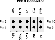
Note that the PPDO bus is an instance of the DAQ_IF SPI bus with a single chip/board select line (BS0). The PPDO bus presumes that there is a single shift register device hooked up to it (e.g., PPRelay-12 looks like a 16-bit shift regster). The size (in bits) of the shift register is arbitrary. In the DAQ system, each PPRelay-12 or PPSSR-16 board you daisy chain to the PPDO connector adds 16 bits to the size of the shift register. For example, if you have two PPRelay-12 and one PPSSR-16 boards daisy-chained to the PPDO connection, the shift register length is 48 bits (16 bits per board).
If you look at the design of the PPRelay-12 (or PPSSR-16) board, you'll discover that it has two TPIC6B595 serial-in/parallel-out shift registers. The MOSI (Master Out, Slave In -- the PPRelay-12 is a slave) signal coming in on the PPDO In connector is fed to the serial in pin on the first TPIC6B595 shift register. The serial out pin on the first TPIC6B595 shift register goes to the serial in pin on the second TPIC6B595. Finally, the serial out pin on the second TPIC6B595 shift register goes to the MOSI pin on the PPDO Out connector. Therefore, if you shift 48 bits onto the PPDO bus, the last 16 bits you shift will wind up on the first board in the daisy chain; the second 16 bits (the middle 16 bits) you shift in will wind up on the second board in the daisy chain; the first set of 16 bits you shift in wind up on the third board in the daisy chain.
Note that the PPRelay-12 and PPSSR-16 boards do not use the MISO, J238, and IRQ signals. The PPRelay-12 and PPSSR-16 boards are output-only devices, so the MISO (Master input, slave output) pin has no use. Likewise, these two boards don't generate any interrupts, so these boards don't use the IRQ line. The DAQ system reserves the J238 line for end-user use, so the PPRelay-12 and PPSSR-16 boards don't use this pin.
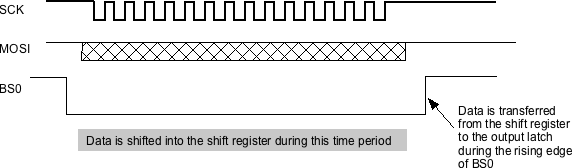
The PPRelay-12 board uses the SCK and MOSI lines to shift data into the shift registers. Although the TPIC6B595 high-current shift registers the PPRelay-12 board uses is not, technically speaking, an SPI device, it turns out that the timing of the SPI clock (SCK) and MOSI (serial output data) signals are compatible with the serial shift clock and serial data in pins on the TPIC6B595 shift register.
Programming PPRelay-12 (PPDO Bus)
Note: Keep in mind that mechanical relays are mechanical. This means that you cannot program a relay to open or close and expect the result to immediately filter through the hardware. The data sheet for the relays the PPRelay-12 board uses states a 20 msec operate time. You can probably assume that as the relay gets older, it may take longer to actuate. You probably shouldn't assume the relay closes any faster than 50 msec, and 100 msec is probably a better assumption. See the data sheet for more details.
As mentioned earlier, the boards daisy-chained to the PPDO connector look like a single shift register to the DAQ_IF board. Adding more PPRelay-12 or PPSSR-16 boards to the daisy chain extends the size of the shift register by 16 bits for each board you add.
To program this "shift register" you must first pull the BS0 line low on the DAQ_IF board. You accomplish this by programming the A0, A1, and A2 output pins (on the DAQ_IF) with zeros and then activate the SPI chip select line. Next, you transmit the specified number of bytes (two bytes for each board in the daisy chain) via the SPI libraries (note: the bit on MOSI gets shifted in on the rising edge of SCK -- this is handled by the SPI libraries or hardware). Finally, you set the BS0 line high (by setting the SPI chip select line high or by writing all ones to the A0, A1, and A2 output lines). On the rising edge of the BS0 signal line, the TPIC6B595 shift registers transfer the data from the internal shift registers to the output latches. Note that during the shift operation, the data on the TPIC6B595 output pins (controlling the relays) does not change until the rising edge of the BS0 signal.
Note: here is some sample code (written for the Netburner) to control the A0, A1, and A2 lines that control BS0:
// disable and enable the board select lines
// for the MCP23s17 chips.
//
//  Note:   board zero is reserved for the
//          DO24 board (serial shift
//          register board).

void disableDIO( void )
{
    // Disable by selecting Y7 on the 74HC138.
    // Y7 is unused by the DIO96 and DO24 boards.

    A0Pin()         = 1;    // A pin on '138
    A1Pin()         = 1;    // B pin on '138
    A2Pin()         = 1;    // C pin on '138
}


// enableDIO-
//
//  Enables the SPI CS line specified by the argument.
//
//  board:  0 for PPDIO bus, 1-6 for PPDIO96 buss,
//          7 for disabled

void enableDIO( BYTE board )
{

    switch( board )
    {
        case 0:
            A0Pin() = 0;    // DOUT boards
            A1Pin() = 0;
            A2Pin() = 0;
            break;


        case 1:
            A0Pin() = 1;    // Board 1
            A1Pin() = 0;
            A2Pin() = 0;
            break;


        case 2:
            A0Pin() = 0;    // Board 2
            A1Pin() = 1;
            A2Pin() = 0;
            break;

        case 3:
            A0Pin() = 1;    // Board 3
            A1Pin() = 1;
            A2Pin() = 0;
            break;

        case 4:
            A0Pin() = 0;    // Board 4
            A1Pin() = 0;
            A2Pin() = 1;
            break;

        case 5:
            A0Pin() = 1;    // Board 5
            A1Pin() = 0;
            A2Pin() = 1;
            break;

        case 6:
            A0Pin() = 0;    // Board 6
            A1Pin() = 1;
            A2Pin() = 1;
            break;


        default:

            // If bad address, disable the chip selects:

            disableDIO();
            return;

    } // switch
} // enableDIO
Here is some comparable code running on a Teensy 3.2 (Arduino style programming):
 void setBSAdrs( int adrs )
{
    if( adrs <0 || adrs > 6 )
    {
        adrs = 7;
    }
    digitalWrite( a0, adrs & 1 );
    digitalWrite( a1, (adrs >> 1) & 1 );
    digitalWrite( a2, (adrs >> 2) & 1 );
    if( adrs == 7 )
    {
        digitalWrite( spics, 1 );
    }
    else
    {
        digitalWrite( spics, 0 );
    }
} // setBSAdrs


void disableAdrs( void )
{
    digitalWrite( spics, 1 );
    digitalWrite( a0, 1 );      // ADRS 7 is unused on DAQ
    digitalWrite( a1, 1 );
    digitalWrite( a2, 1 );
} // setBSAdrs
Here is some Teensy 3.2 library code that writes 16 bits to the SPI bus (the exact code varies by SBC). Note that "RelaySettings" is the SPISettings object created in the Teensy code to communicate with the SPI bus.
SPISettings RelaySettings; //( 2000000, MSBFIRST, SPI_MODE1 );


void transferWord( uint16_t word )
{
        setBSAdrs( 0 );
        SPI.beginTransaction( RelaySettings );
        SPI.transfer( word >> 8 );
        SPI.transfer( word & 0xff );
        SPI.endTransaction();
        disableAdrs();
}
So if you wanted to write the 48 bits "0x0000, 0x1f00, 0x8000" to three PPRelay-12 boards attached to the DAQ_IF, you'd use the following Teensy 3.2 code
        setBSAdrs( 0 );
        SPI.beginTransaction( RelaySettings );
        SPI.transfer( 0x80 );       // H.O. byte of 0x8000
        SPI.transfer( 0x0 );        // L.O. byte of 0x8000
        SPI.transfer( 0x1f );       // H.O. byte of 0x1f00
        SPI.transfer( 0x0 );        // L.O. byte of 0x1f00
        SPI.transfer( 0x0 );        // H.O. byte of 0x0
        SPI.transfer( 0x0 );        // L.O. byte of 0x0
        SPI.endTransaction();
        disableAdrs();
Note that you must transfer the H.O. byte of each word first.
Because of the nature of shift registers, if you shift extra data to the shift registers (more than n*2 bytes, where n is the number of daisy-chained boards) then the extra data is lost (the extra data will be the first bytes you shift out). Because of the wiring of the daisy-chain, the last two data bytes you shift out will be shifted into the first board in the daisy chain (the board connected directly to the DAQ_IF board), the two bytes shifted out before the last two bytes will be shifted into the second board of the daisy chain, etc.
Toggling the DAQ_IF reset line will immediately clear all the TPIC6B595 shift registers and output latches. While the reset line is low, the PPRelay-12 and PPSSR-16 boards will force the internal shift registers to all zero bits. On the rising edge of the reset line, the boards will transfer the data (now zeros) from the internal shift registers to the output latches. Note that if you are in the middle of shifting data into the shift registers while also pulsing the reset line (say, in a multi-threaded environment), the results are undefined. If you must shift data into the shift register from one thread and you could be toggling the reset line from a separate thread, you should use synchronization primitives to protect access to the SPI clock.
Here is the Teensy 3.2 code that will toggle the reset line:
#define reset           23

void toggleReset( void )
{
    digitalWrite( reset, 0 );
    delay( 3 );
    digitalWrite( reset, 1 );
    delay( 3 );
}
Here is the Netburner code that will toggle the reset line:
#define RESET 				(J2[44])

// Reset the DAQ system hardware (put system in fail-safe mode:

void reset( void )
{

    // Note: as per requirements, pulse should be low for
    // at least 200 mSec.

    RESET = 1;
    OSTimeDly(2);
    RESET = 0;
    OSTimeDly(2);
    RESET   = 1;
    OSTimeDly(1);
}
Note that DAQ system requirements state that the RESET line must be held low for at least 250 msec. This is why the large delays are present in this code.
If the watchdog timer times out and asserts the WD signal on the PPDO connector, the PPRelay-12 board will automatically put the output relays in a fail-safe mode by clearing the internal shift register and transferring their contents to the TPIC6B595 output latches. As for the reset line, if you're currenting shifting data into the shift register when the WD timer times out, this could create an undefined result. In theory, the software has hung up and probably isn't shifting data to the PPDO connector. In practice, this could be the result of some operation taking too long. To prevent this undefined operation, it's a good idea to always refresh the watchdog timer immediately prior to shifting out any data and checking the WD_LATCH value to ensure that the watchdog timer hasn't already timed out.
Here's some sample Teensy 3.2 code that will refresh the watchdog timer:
#define wd_rfsh         17

void refreshWD( void )
{
    digitalWrite(wd_rfsh, HIGH );
    delayMicroseconds( 10 );
    digitalWrite( wd_rfsh, LOW);
    delayMicroseconds( 10 );
}
Here is the Netburner MOD54415 code that will refresh the watchdog timer:
#define RESET 				(J2[44])

			led1Pin()	= 0;
         shortDelay(10);
			led1Pin()	= 1;

// shortDelay is defined thusly:
//
// Software delay function (arg in microseconds)

void shortDelay( unsigned int usec )
{
    unsigned int i;

    i = 20*usec;    // 20=1usec delay (approx)
    do
    {
        i--;
        asm("nop"); //needed so delay not optimized out
    }while( i>0);
}